


Non-contact IV tester

Quantum Efficiency Tester
PL/EL Integrated System
PV-Reflectumeter
3D Confocal Microscope
In-Line Four Point Probe Tester
Four Point Probe Tester
In-Line Thin Film Thickness Tester
Raman Spectrometer
FTIR Spectrometer
Spectrophotometer
Automatic Spectroscopic Ellipsometer
Contact Resistance Tester
Ultra depth of field 3D microscope
Auto Visual Tester
VMM PV Vision Measuring Machine
Solar Cell Horizontal Tensile Tester
Steady State Solar Simulator for Solar Cell
Solar Cell UV Aging Test Chamber
Solar Cell Comprehensive Tensile Tester
Visual Inspection Tester
Wet Leakage Current Tester
PV Module EL Tester
PV Module UV Preconditioning Chamber
Steady State Solar Simulator for PV Module
Current Continuous Monitor
Potential Induced Degradation Test
Bypass Diode Tester
LeTID Test System
Reverse Current Overload Tester
Impulse Voltage Tester
Hipot Insulation Tester
Ground Continuity Tester
Hipot Insulation Ground Tester
Damp Heat Test Chamber
Humidity Freeze Test
Thermal Cycle Test Chamber
Dynamic Mechanical Load Tester
Static Mechanical Load Tester
Hail Impact Tester
Robustness of Termination Tester
Module Breakage Tester
Cut Susceptibility Tester
Peel Shear Strength Tester
Universal Testing Machine (Single-arm)
Universal Testing Machine (Double-arm)
Glass Transmittance Tester
Acetic Acid Test Chamber
EVA Degree of Crosslinking Test System
Junction Box Comprehensive Tester
Drop ball tester
Semi-automatic scanning four-probe tester
Stylus Profilometer
Maximum Power Point Tracker
Perovskite Glass Transmittance Tester
Perovskite P1 Laser Scribing Multifunctional Testing Machine
Perovskite Online PL Tester
Perovskite Online Sheet Resistance Tester
Online Perovskite Film Thickness Tester
Perovskite Process Inspection Workstation
Portable EL Tester
Portable Thermal Imaging Tester
Solar Module Multi-Channel Testing System
PV Inverter Power Quality Tester
IV Tester
IVEL Cell Sorting Machine
Radiation-Resilient Wide-Bandgap Perovskite/Silicon Tandem Solar Cells for Space Photovoltaics with 27.49% AM0 Efficiency
Date : 21 October 2026Views : 35
The rapid deployment of low-Earth-orbit satellite constellations is raising the requirements for space photovoltaics in three areas: high efficiency, low cost, and long service life. III–V solar cells offer strong performance but are expensive; silicon cells are relatively inexpensive but have limitations in specific power and radiation resistance; and single-junction perovskite cells generally achieve limited efficiency under AM0 illumination. Perovskite/silicon tandem cells offer a route beyond these efficiency limitations, but monolithic integration presents a key challenge: radiation damage to the silicon bottom cell reduces the efficiency of the entire tandem device. Radiation tolerance depends strongly on whether p-type or n-type silicon is used and on silicon thickness, with conventional n-type silicon showing substantial degradation under space irradiation.Millennial Solar Perovskite Maximum Power Point Tracker (MPPT) uses a Class 3A+ LED solar simulator as an aging light source and enables temperature and atmospheric control for long-term stability testing.
This study developed a radiation-resilient monolithic tandem architecture combining a 1.72 eV wide-bandgap perovskite top cell with a 100 μm-thick p-type silicon heterojunction bottom cell. The inherent radiation tolerance of p-type silicon helps mitigate bottom-cell degradation. An ionic-liquid additive, [Bcmim]Cl, was also introduced to improve perovskite film quality and suppress phase segregation and nonradiative recombination. This design improves current matching under the AM0 spectrum while enhancing device tolerance to the space environment.
The top cell was fabricated in a p-i-n configuration (ITO/SAM/perovskite/C₆₀/BCP/Ag) using a Cs₀.₂₂FA₀.₇₈Pb(I₀.₈Br₀.₂)₃ precursor, with [Bcmim]Cl added before spin coating. The bottom cell was fabricated on a textured, 100 μm-thick p-type monocrystalline silicon wafer, incorporating amorphous-silicon/nanocrystalline-silicon passivation layers and an IWO transparent electrode. The monolithic tandem was built sequentially on p-Si: a 10 nm IWO recombination interlayer was deposited, followed by the perovskite top cell, C₆₀, SnOₓ, ITO, silver gridlines, and finally an evaporated MgF₂ layer.
Irradiation tests used 1 MeV electrons and 150 keV protons at graded fluences. CASINO and SRIM simulations were used to examine energy deposition and damage distributions. Films were characterized by SEM, GIWAXS, AFM, KPFM, SCLC, PL, and QFLS measurements. AM0 performance was independently certified at 1353 W/m²; bidirectional J–V scans were performed under both AM1.5G (1000 W/m²) and AM0 (1353 W/m²). For near-space validation, an encapsulated 12.56 cm² tandem device, laminated using cover glass, space-grade silicone, and SiOₓ, was mounted on a high-altitude balloon payload for in-flight I–V measurements under actual near-space illumination and low-pressure conditions.
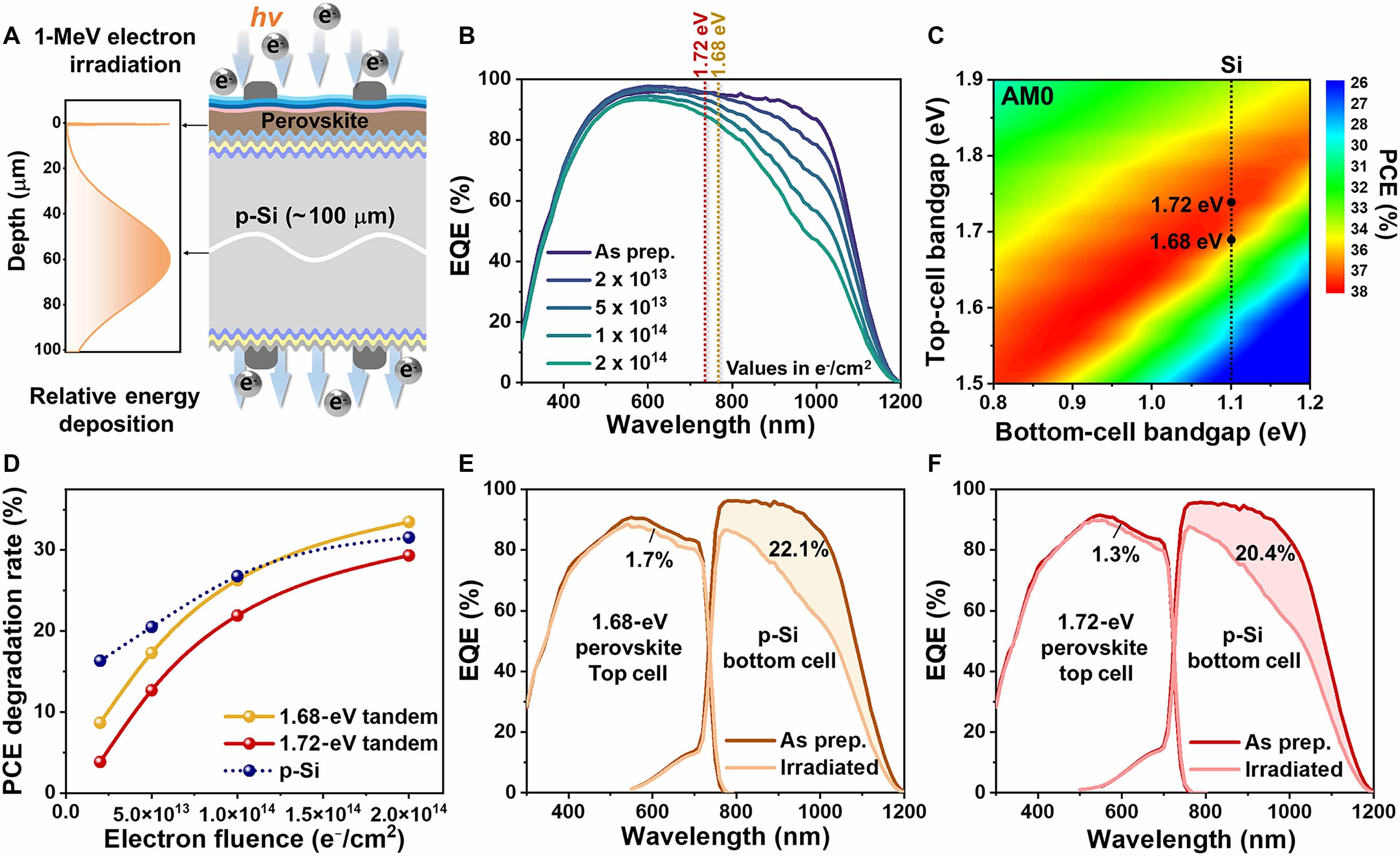
Electron irradiation tolerance of monolithic perovskite/silicon tandem cells with different top-cell bandgaps
Simulations indicated that most of the energy from 1 MeV electron irradiation was deposited in the silicon bottom cell. Measurements supported this finding: at an electron fluence of 2 × 10¹⁴ e⁻/cm², n-type silicon cell efficiency declined by 97.58%, compared with 31.8% for p-type silicon. This substantial difference highlights the greater radiation tolerance of p-type silicon. EQE measurements also showed reduced long-wavelength response after irradiation, consistent with an increase in bulk defects.
Increasing the top-cell bandgap from the commonly used 1.68 eV to 1.72 eV improved current matching with the irradiated silicon bottom cell under AM0 illumination. After 1 × 10¹⁴ e⁻/cm² electron irradiation, the 1.72 eV tandem retained approximately 80% of its initial efficiency, compared with 73% for the 1.68 eV device. The 1.72 eV top cell initially generates less current, resulting in better matching after the silicon bottom-cell current decreases.
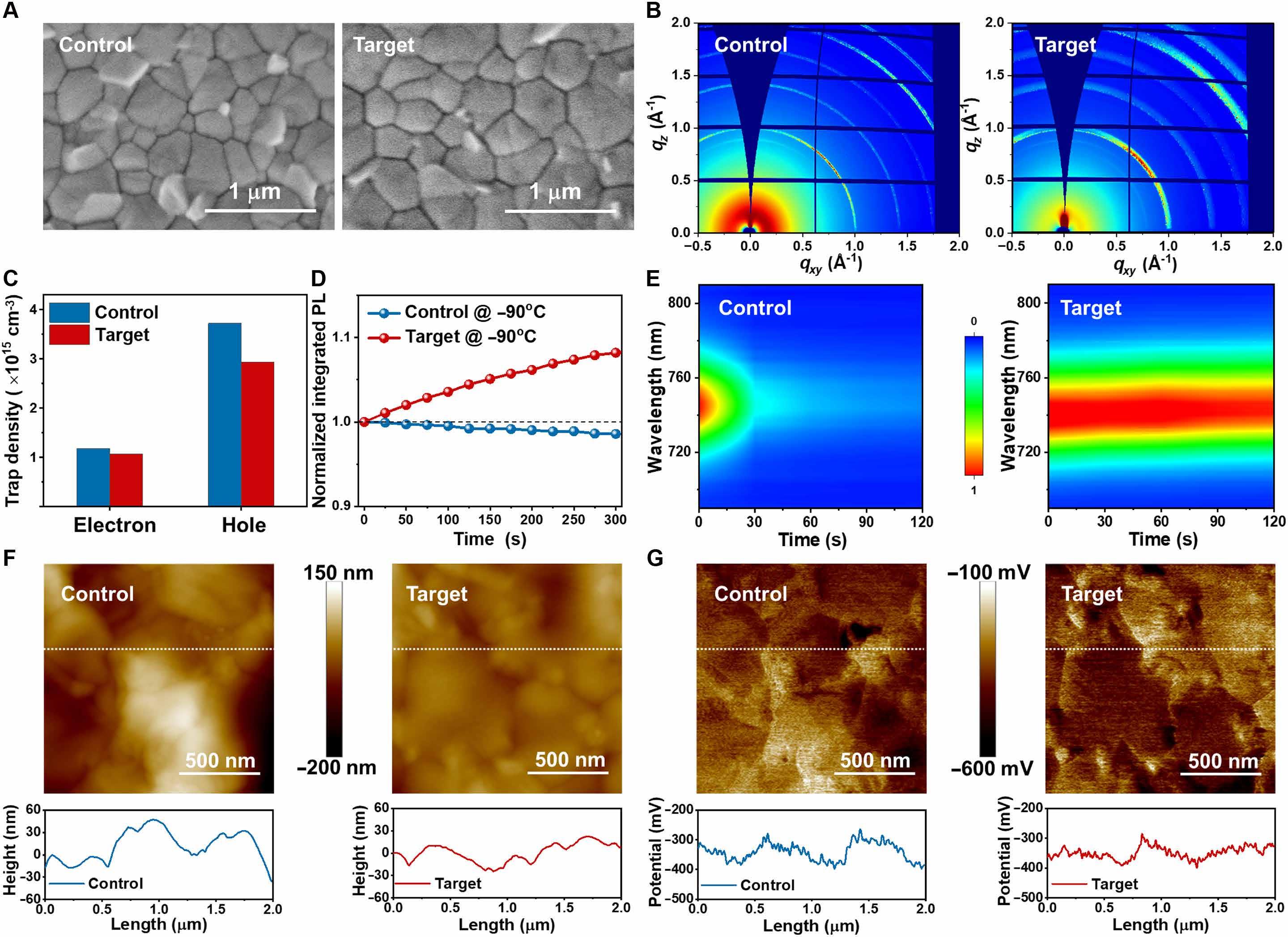
Characterization of 1.72 eV wide-bandgap perovskite films with and without the [Bcmim]Cl additive
Wide-bandgap perovskites (>1.70 eV) are susceptible to phase segregation and nonradiative recombination. The study introduced [Bcmim]Cl to address these challenges. Characterization showed that the additive increased grain size, improved crystallographic orientation, and reduced film surface roughness. SCLC measurements indicated lower electron and hole trap densities. KPFM revealed an upward shift in the perovskite surface Fermi level, improving energy-level alignment with the electron transport layer. PL measurements showed greater stability of additive-treated films under low-temperature conditions, continuous illumination, and combined high-temperature/illumination aging, with suppressed halide phase segregation and defect formation.
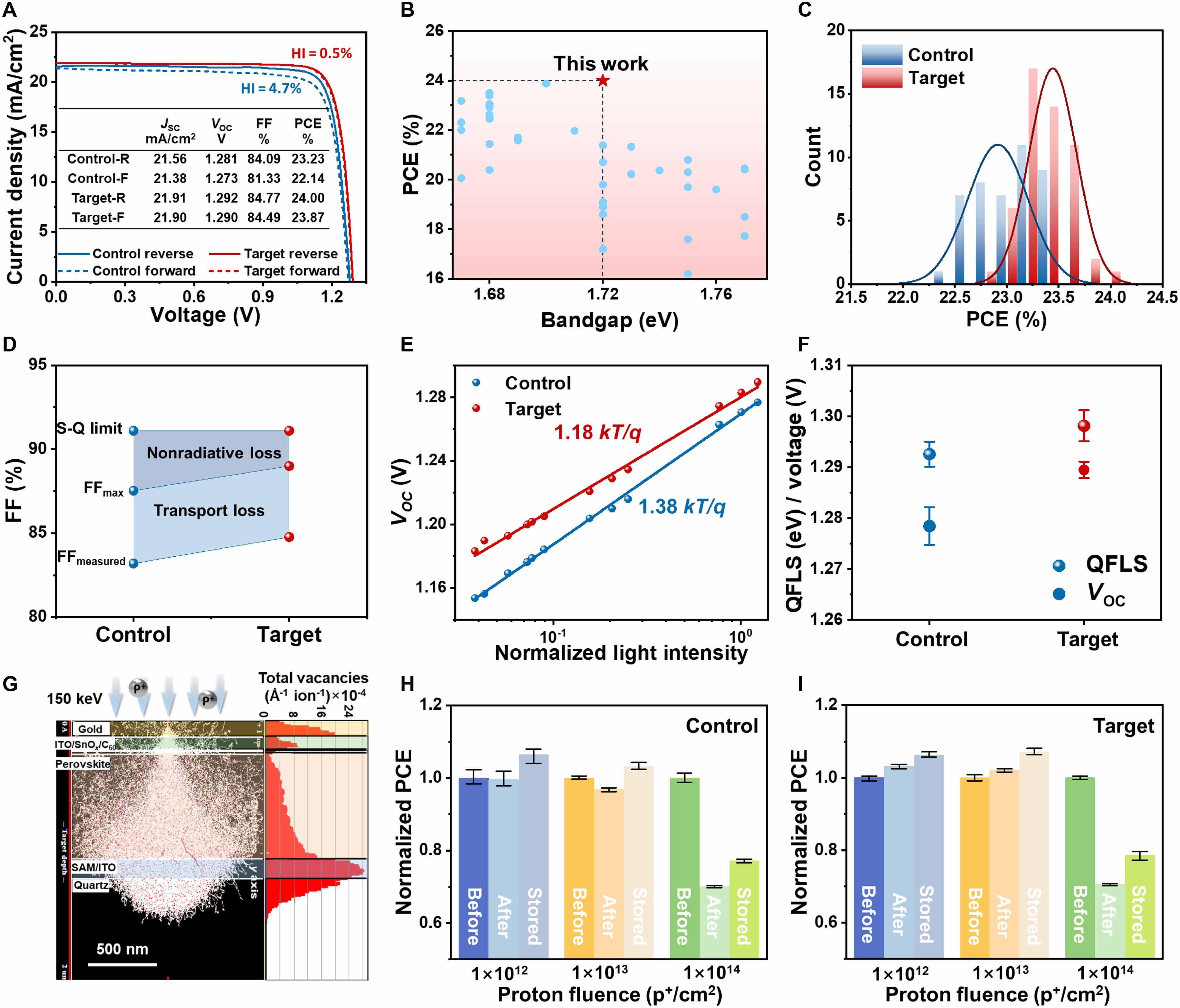
Photovoltaic performance and stability improvements enabled by the [Bcmim]Cl additive
For single-junction cells fabricated using the optimized 1.72 eV perovskite, efficiency increased from 23.23% to 24.00% (with a certified efficiency of 23.58%). The target devices showed substantially reduced hysteresis and ideality factor, increased QFLS, and suppressed nonradiative recombination. Under illuminated aging at 85°C and low-temperature testing at −90°C, the target devices exhibited markedly better stability than the control devices.
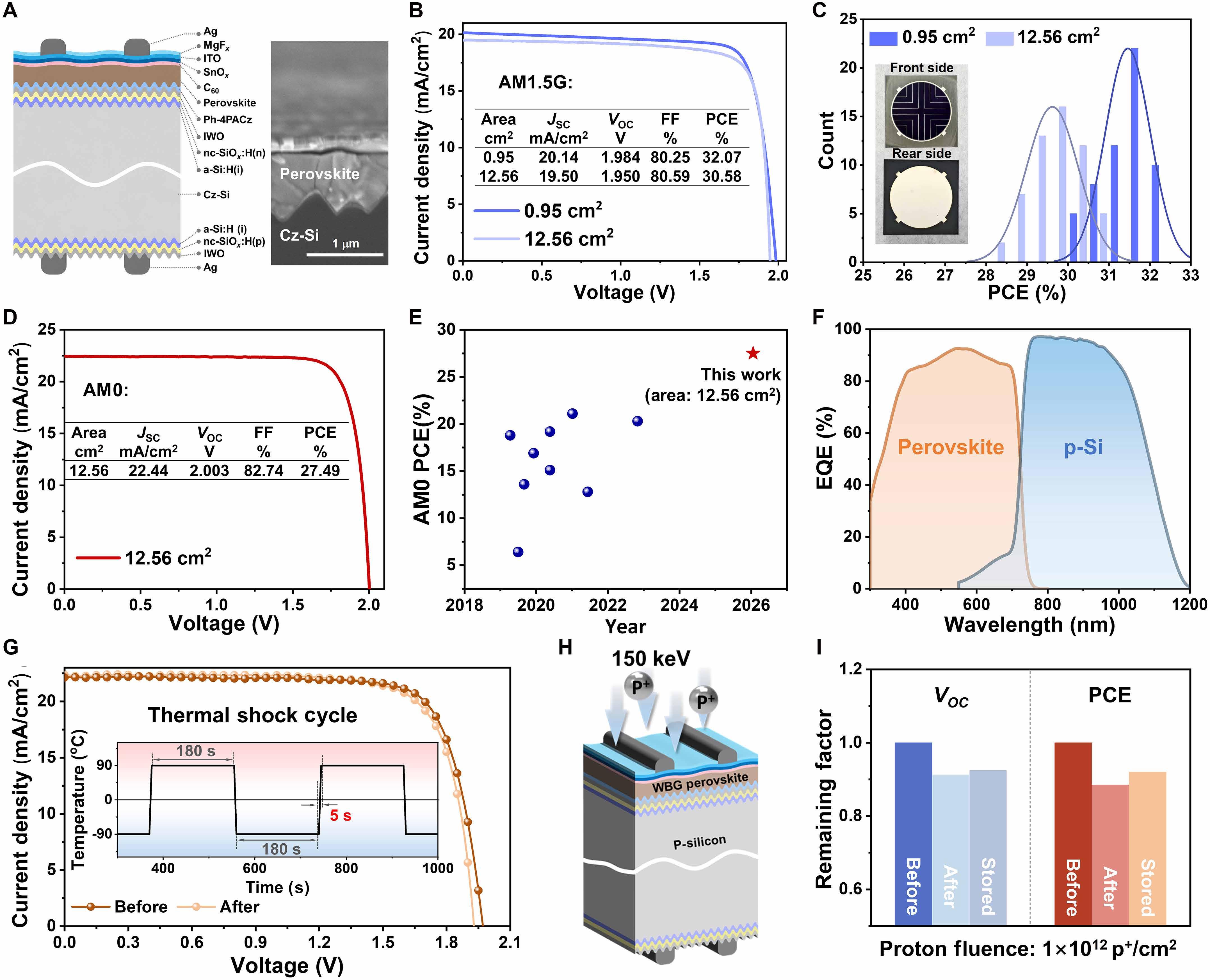
Device performance of wide-bandgap perovskite/p-Si tandem solar cells
Under 150 keV proton irradiation, the target devices exhibited a pronounced self-recovery effect at low fluences, with efficiency recovering after five days of dark storage and outperforming the control devices. By contrast, single-junction silicon devices suffered substantial degradation after proton irradiation without recovery.
The fabricated tandem devices achieved AM1.5G efficiencies of 32.07% for the small-area cell (0.95 cm²) and 30.58% for the large-area cell (12.56 cm²). The large-area device achieved a certified AM0 efficiency of 27.49%, reported in the source article as the highest certified AM0 efficiency for a perovskite/silicon tandem cell at the time. EQE-derived currents showed close current matching between the top and bottom subcells under AM0 illumination.
Regarding environmental durability, the devices retained 96.8% of their efficiency after thermal-shock cycling from −90°C to 90°C, 93% after 150 keV proton irradiation, and approximately 95% of their initial efficiency after 550 hours of damp-heat aging
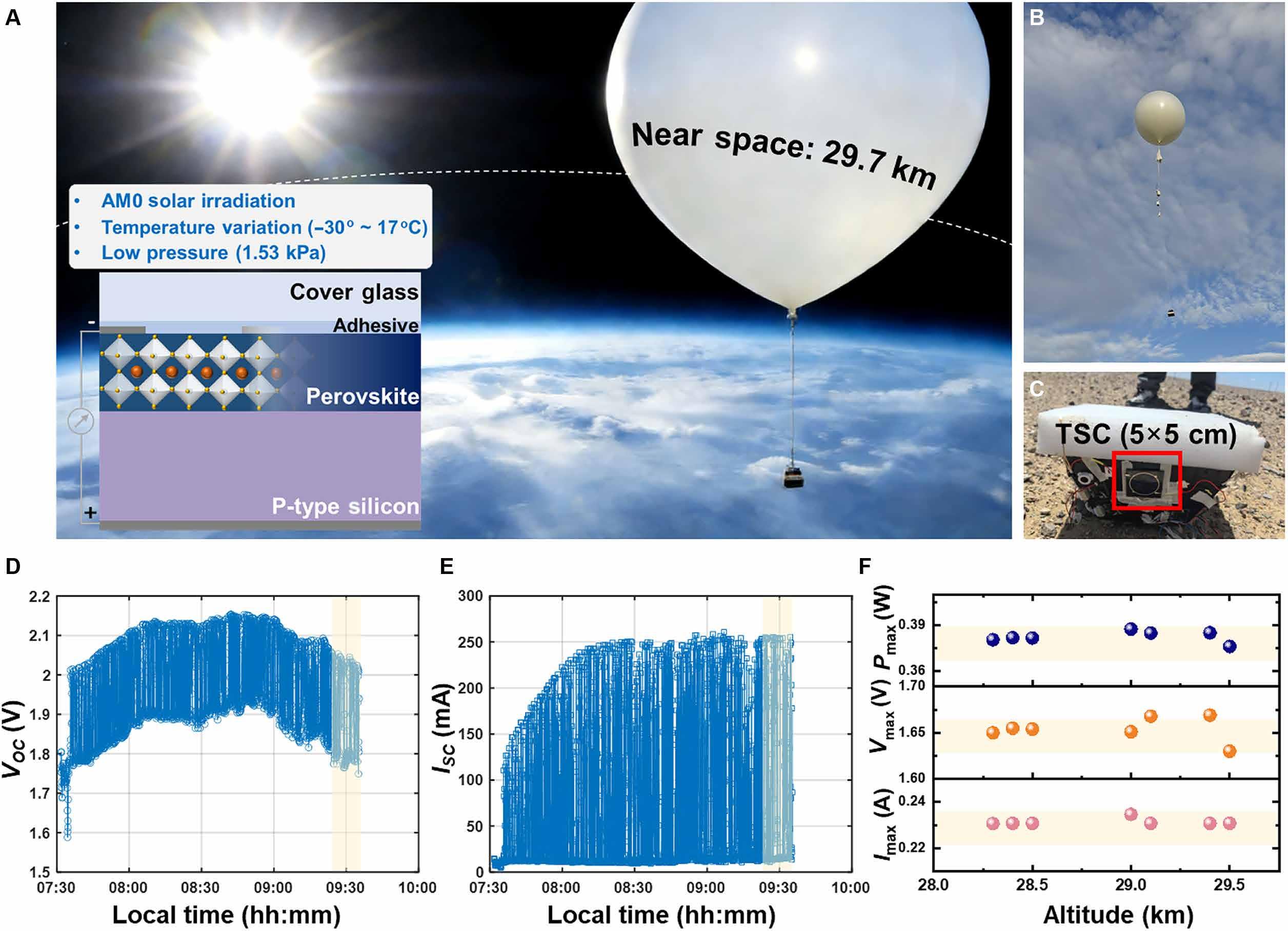
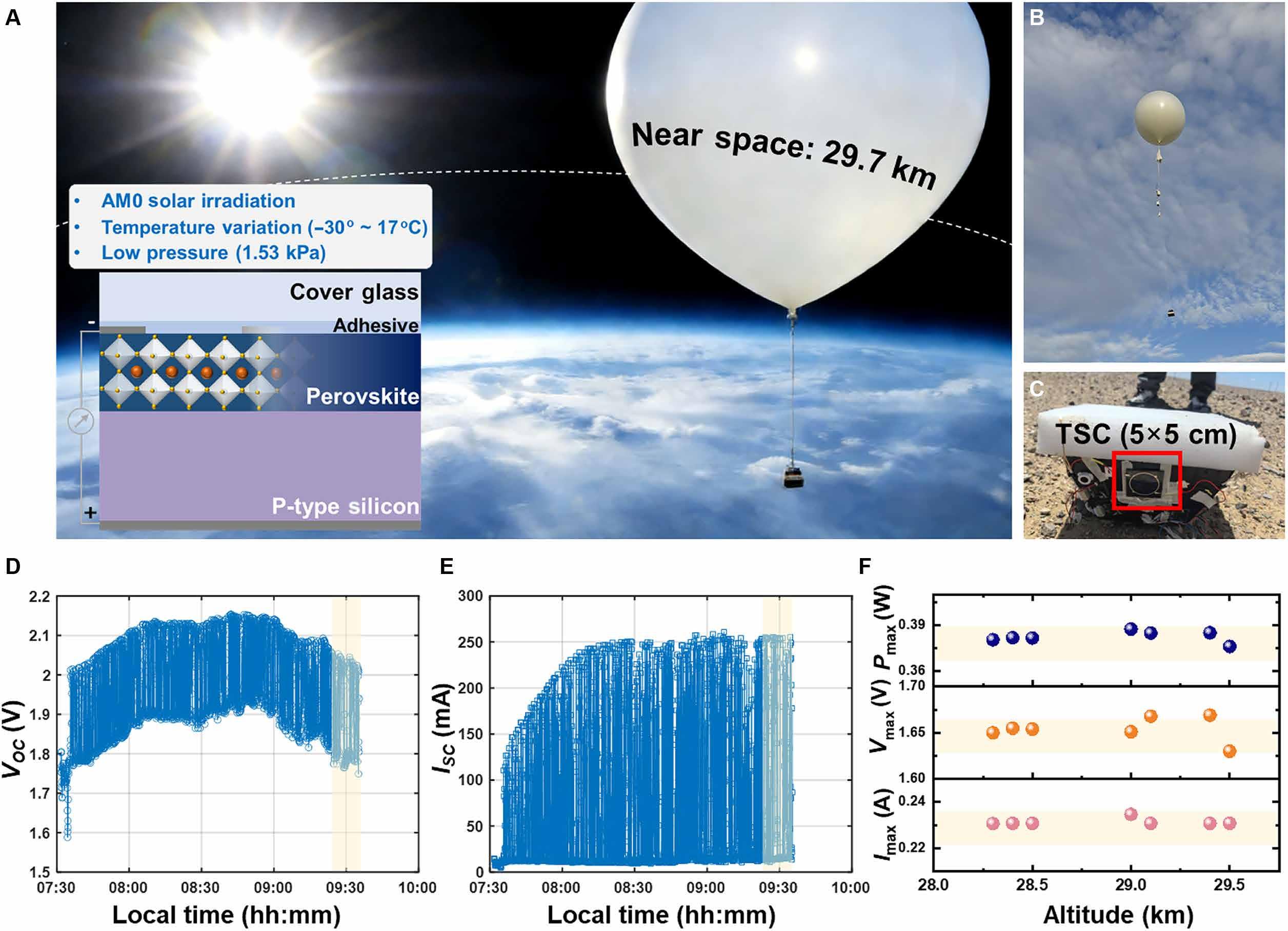
High-altitude balloon platform for in-situ monitoring of wide-bandgap perovskite/p-Si tandem devices in near space
To evaluate device operation under actual near-space conditions, the research team carried encapsulated devices to an altitude of approximately 29.7 km using a high-altitude balloon. During flight, Voc and Isc remained largely stable, with minor variations associated with the illumination angle. During the relatively stable flight segment between 28.3 and 29.7 km, reproducible I–V curves were obtained over several measurement periods, and the maximum output power reached 387.4 mW. No progressive performance loss or I–V curve distortion was observed during the flight, supporting the performance of the encapsulation and device architecture under the tested near-space conditions.
By combining bandgap tuning, additive-enabled stabilization, and a radiation-tolerant silicon bottom cell, this study demonstrated a radiation-resilient monolithic wide-bandgap perovskite/p-Si tandem device. The 1.72 eV top cell improved AM0 current matching; [Bcmim]Cl reduced trap-related losses and phase segregation while enhancing thermal and light stability; and the thin p-type silicon bottom cell provided greater tolerance to electron and proton irradiation.
The device achieved 27.49% certified AM0 efficiency, retained nearly 80% of its initial efficiency after 1 MeV electron irradiation and 93% after 150 keV proton irradiation, and delivered a stable maximum output power of 387.4 mW during near-space flight. The approach addresses three major challenges for space tandem photovoltaics—AM0 spectral mismatch, environmental instability of wide-bandgap materials, and radiation-induced degradation—and offers a potentially scalable photovoltaic route for orbital platforms, satellite arrays, and planetary surface missions.
The 12.56 cm² tandem device achieved a certified AM0 efficiency of 27.49% under 1353 W/m² illumination.
Q2: How did the device perform under electron and proton irradiation?The 1.72 eV tandem retained approximately 80% of its initial efficiency after 1 MeV electron irradiation at 1 × 10¹⁴ e⁻/cm² and 93% after 150 keV proton irradiation.
Q3: Was the tandem solar cell tested in near-space conditions?Yes. During a high-altitude balloon flight reaching approximately 29.7 km, the encapsulated device produced reproducible I–V curves and reached a maximum output power of 387.4 mW.
Email: market@millennialsolar.com
The Millennial Solar Perovskite Maximum Power Point Tracker (MPPT) uses a Class 3A+ LED solar simulator as an aging light source. Compared with the previous generation, its spectral range has been extended to 300–1700 nm (AM0), its spectral classification reaches AAA (AM0), and it supports 24 independently adjustable channels. These features support research on perovskite solar cells, space photovoltaics, and tandem cells (2T/3T/4T).
▶ Light source classification: AAA (AM0), with a spectral range of 300–1700 nm for space photovoltaic testing.
▶ Independently adjustable spectral bands: 24 adjustable channels (AM0) for matching the subcell bandgaps of triple- and quadruple-junction tandem cells.
▶ Large-area sample fixture: Supports tandem cells up to 210 × 105 mm, with front- and rear-side gold-wire pressure contacts for electrode connection.
▶ Environmental control: Semiconductor-based temperature control from 15°C to 100°C, with testing available in a nitrogen atmosphere free of moisture and oxygen.
The Millennial Solar perovskite MPPT testing system serves not only as a performance verification tool but also as a testing platform for perovskite and tandem solar-cell research.
Original Research Reference: Radiation-resilient monolithic wide-bandgap perovskite/p-type heterojunction silicon tandem solar cells for space photovoltaics
Related Products


