


Non-contact IV tester

Quantum Efficiency Tester
Accurate EQE, IQE and spectral response measurements—from localized spots to full cells.
The MNPVQE-1800T PRO is designed for photovoltaic research and production, providing accurate measurements of solar cell spectral response, external quantum efficiency (EQE/IPCE) and internal quantum efficiency (IQE). The MNPVQE-1800T PRO supports a wide range of photovoltaic devices, including crystalline silicon, multicrystalline silicon, amorphous silicon, microcrystalline silicon, CdTe, CIGS, CIS, Ge, dye-sensitized, organic/polymer, tandem, multijunction, quantum-well, quantum-dot, chalcogenide and perovskite solar cells.PL/EL Integrated System
PV-Reflectumeter
3D Confocal Microscope
In-Line Four Point Probe Tester
Four Point Probe Tester
In-Line Thin Film Thickness Tester
Raman Spectrometer
FTIR Spectrometer
Spectrophotometer
Automatic Spectroscopic Ellipsometer
Contact Resistance Tester
Ultra depth of field 3D microscope
Auto Visual Tester
VMM PV Vision Measuring Machine
Solar Cell Horizontal Tensile Tester
Steady State Solar Simulator for Solar Cell
Solar Cell UV Aging Test Chamber
Solar Cell Comprehensive Tensile Tester
Visual Inspection Tester
Wet Leakage Current Tester
PV Module EL Tester
PV Module UV Preconditioning Chamber
Steady State Solar Simulator for PV Module
Current Continuous Monitor
Potential Induced Degradation Test
Bypass Diode Tester
LeTID Test System
Reverse Current Overload Tester
Impulse Voltage Tester
Hipot Insulation Tester
Ground Continuity Tester
Hipot Insulation Ground Tester
Damp Heat Test Chamber
Humidity Freeze Test
Thermal Cycle Test Chamber
Dynamic Mechanical Load Tester
Static Mechanical Load Tester
Hail Impact Tester
Robustness of Termination Tester
Module Breakage Tester
Cut Susceptibility Tester
Peel Shear Strength Tester
Universal Testing Machine (Single-arm)
Universal Testing Machine (Double-arm)
Glass Transmittance Tester
Acetic Acid Test Chamber
EVA Degree of Crosslinking Test System
Junction Box Comprehensive Tester
Drop ball tester
Semi-automatic scanning four-probe tester
Stylus Profilometer
Maximum Power Point Tracker
Perovskite Glass Transmittance Tester
Perovskite P1 Laser Scribing Multifunctional Testing Machine
Perovskite Online PL Tester
Perovskite Online Sheet Resistance Tester
Online Perovskite Film Thickness Tester
Perovskite Process Inspection Workstation
Portable EL Tester
Portable Thermal Imaging Tester
Solar Module Multi-Channel Testing System
PV Inverter Power Quality Tester
IV Tester
IVEL Cell Sorting Machine
Trans-Interface Engineering Enables 27.04%-Efficient Perovskite Solar Cells with Reproducible Stability
Date : 19 November 2026Views : 25
Degradation in perovskite solar cells is concentrated at device interfaces, where chemical degradation and mechanical failure can occur simultaneously. Chemical degradation is temperature-dependent and can be predicted thermodynamically. Mechanical failure, however, results from interfacial delamination caused by voids and cracks. Its sudden and stochastic nature can cause unpredictable efficiency drops during operation and makes device-to-device stability difficult to control. Existing interface modifications typically place a planar interlayer between the perovskite and charge transport layer. Such interlayers rely on coordination bonds and hydrogen bonds, provide limited improvement in mechanical adhesion, and do not extend into the charge transport layer. Millennial Solar Maximum Power Point Tracker uses a Class 3A+ LED solar simulator as an aging light source, with temperature and atmospheric control for long-term stability testing.
This study proposes trans-interface engineering (TIE). The trifunctional monomer trimethylolpropane triacrylate (TMTA) was premixed into the perovskite precursor solution, while the monofunctional monomer acrylamide (AM) was introduced into the SnO₂ colloidal solution. Cyanoprop-2-yl radicals generated by thermal decomposition of azobisisobutyronitrile (AIBN) initiated polymerization of both monomers within their respective layers and copolymerization at the perovskite/SnO₂ interface, creating polymer nano-linkages extending vertically through both layers. The champion device achieved a power conversion efficiency of 27.04% (26.67% certified), and 92% of devices reached a T80 lifetime of 1,400 h under maximum power point tracking.
The molecular design of TIE centers on two crosslinkable monomers. TMTA offers high crosslinking density and good water resistance after polymerization, while the hydrophilicity of AM facilitates its incorporation into metal-oxide-based charge transport layers. Upon heating, AIBN decomposes into cyanoprop-2-yl radicals, which react with C=C bonds in both monomers to initiate chain growth. Heating the two monomers with AIBN at 50°C under nitrogen produced PTMTA and PAM through separate polymerization, as well as the copolymer P(AM)m(TMTA)n. To verify copolymerization, a dimethylformamide solution containing TMTA and AIBN was added to prepolymerized PAM. After heat treatment, a two-segment rod-like structure formed. During tensile testing, fracture consistently occurred within the PAM segment rather than at the PTMTA/PAM interface, indicating chemical bonding across the interface.
The devices adopted an n–i–p architecture. TMTA and AIBN were added to the perovskite precursor, and AM was added to the SnO₂ colloidal solution before spin coating. During heat treatment, TMTA polymerized along perovskite grain boundaries, AM polymerized at interfaces between SnO₂ particles, and the two monomers copolymerized at the perovskite/SnO₂ interface. The optimal monomer concentration was 1 mg mL⁻¹. In the control group, TMTA polymerized only within the perovskite layer; the resulting polymer linkages did not cross the perovskite/electron transport layer (ETL) interface. This design isolated the contribution of trans-interface linkages.
Mechanical properties were evaluated using four methods: the ASTM D3359 cross-cut tape adhesion test, nanoscratch testing for critical load, tensile testing for maximum delamination stress, and the double-cantilever-beam method for interfacial toughness. Charge dynamics were investigated using steady-state and time-resolved photoluminescence (TRPL) and space-charge-limited current (SCLC) measurements. All stability tests used PTAA as the hole transport layer, with a glass/ITO/SnO₂/perovskite/PTAA/Au device structure. Unencapsulated devices underwent maximum power point tracking under flowing nitrogen; devices used for damp-heat testing were encapsulated. Stability was assessed under ISOS-L-1, ISOS-L-2, ISOS-T-3, and ISOS-D-3 protocols.
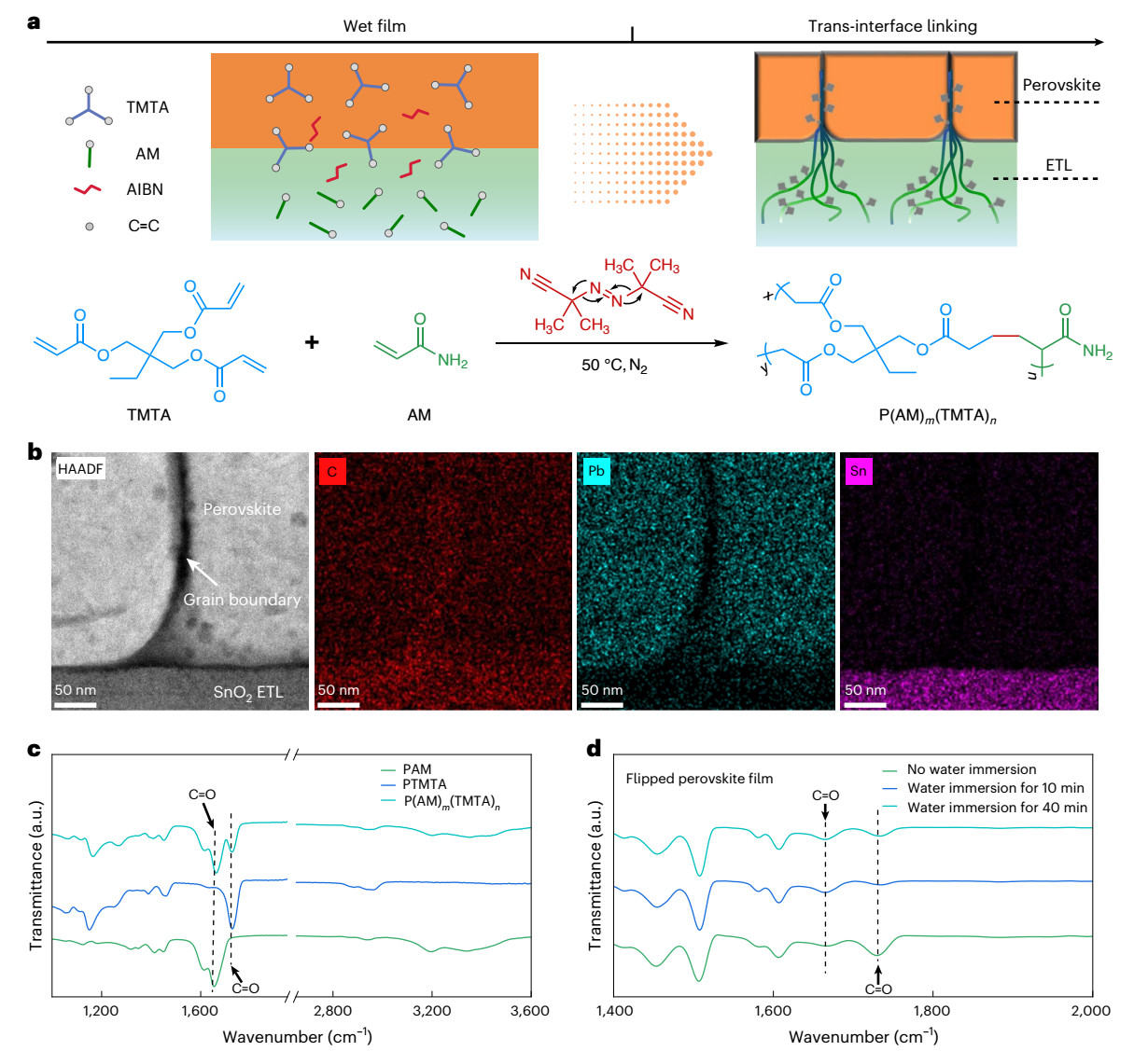
(a) Top: schematic of TIE extending across the entire ETL/perovskite heterointerface of a perovskite solar cell (PSC) at grain-level resolution. Bottom: AIBN-initiated polymerization of AM and TMTA under heat treatment in N₂. (b) Cross-sectional HAADF image of a TIE device with FA₀.₉Cs₀.₁PbI₃ perovskite and corresponding elemental maps (C, Pb, and Sn). (c) FTIR spectra of polymerized PAM, PTMTA, and the P(AM)m(TMTA)n copolymer. (d) FTIR spectra of inverted CsPbI₂Br perovskite films containing TIE after different immersion times in water.
Cross-sectional transmission electron microscopy (TEM) revealed a polymer network at perovskite grain boundaries that extended into the interparticle interfaces of the SnO₂ ETL. Carbon mapping by high-angle annular dark-field scanning transmission electron microscopy (HAADF-STEM) showed an amorphous network connecting perovskite grain boundaries to the SnO₂ ETL. Similar amorphous features were observed across regions with different grain-boundary geometries, indicating that network formation was not dependent on the local interface structure. Rinsing with dimethylformamide provided evidence of solvent resistance: the polymer network in TIE samples remained attached to the SnO₂ ETL after rinsing, whereas no network remained on the ETL when polymerization occurred only in the perovskite or only in the SnO₂ layer.
Fourier-transform infrared spectroscopy (FTIR) provided evidence of chemical linkage. The characteristic C=O peaks of pure TMTA and AM were located at approximately 1,730 cm⁻¹ and 1,655 cm⁻¹, respectively, and both peaks were retained after polymerization. Both peaks also appeared on the underside of inverted CsPbI₂Br perovskite films and remained intact after 40 min of water immersion. CsPbI₂Br was selected to avoid interference from signals associated with FA⁺ and the polymer. Because AM and PAM are water-soluble whereas the copolymer is insoluble, the retained peaks support their assignment to an AM–TMTA copolymerization product.
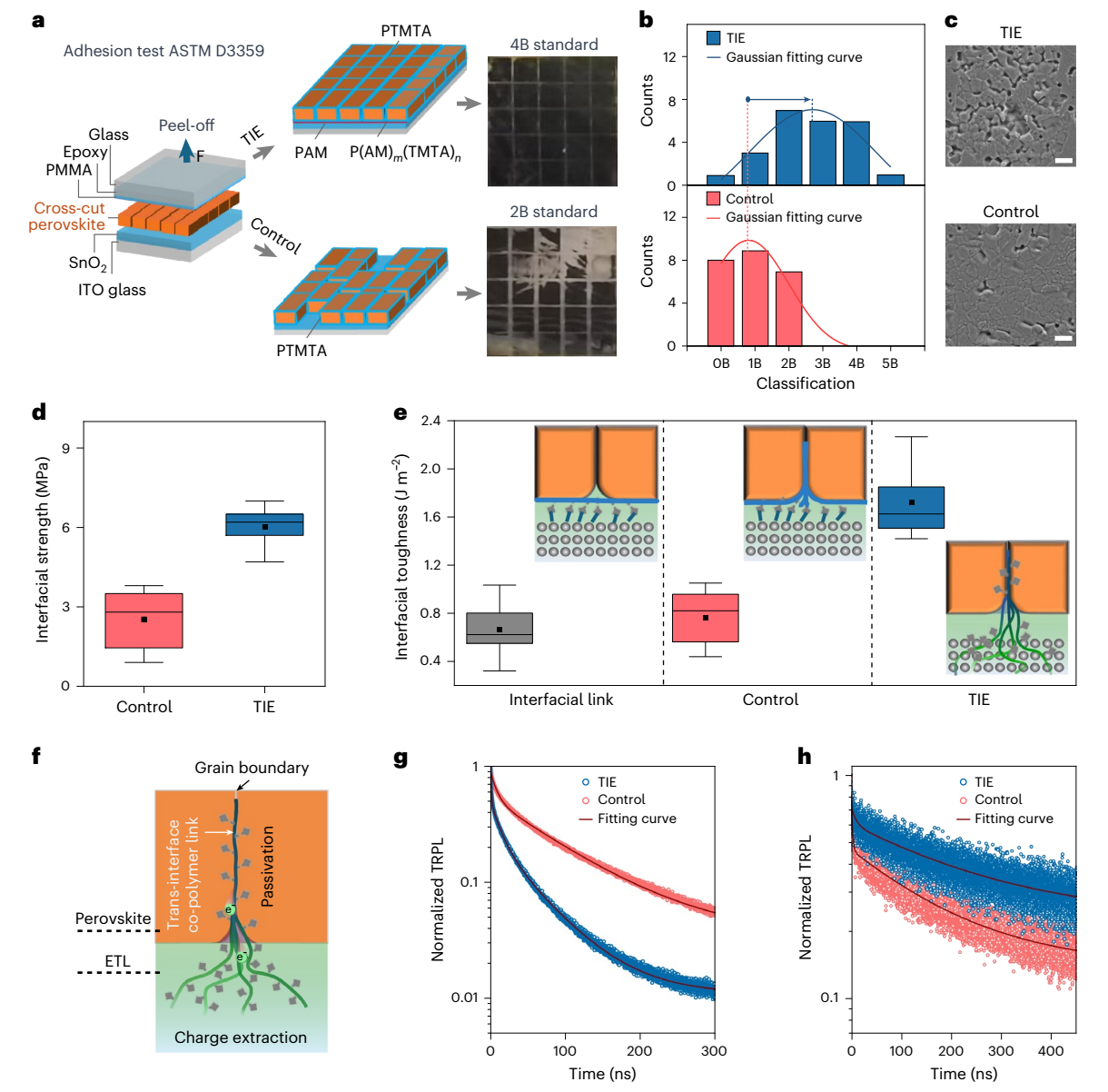
(a) Schematics and adhesion-grade statistics for adhesion tests on different perovskite films. (b) Adhesion and delamination classifications. (c) SEM images of perovskite regions detached from the upper glass substrate. (d) Interfacial strength statistics at the SnO₂/perovskite interface. (e) Interfacial toughness for different interface designs (interfacial linkage, control, and TIE). In (d) and (e), whiskers indicate minimum and maximum values, box edges represent the 25th and 75th percentiles, and center lines indicate means. (f) Schematic of grain-level TIE linkages. (g) TRPL spectra of perovskite films deposited on SnO₂ ETLs with and without TIE. (h) TRPL spectra of control and TIE films peeled from SnO₂-ETL-coated substrates.
Under ASTM D3359, the average adhesion classification for 5 × 5 cross-cut specimens (24 grid areas per film type) improved from 1B in the control (35%–65% of the area affected by delamination) to 3B with TIE (0%–15%). The average critical load in nanoscratch tests increased from 2,239 μN to 2,759 μN. Tensile tests showed an increase in maximum delamination stress from 3.5 to 7.0 MPa; statistics from six samples per group indicated a threefold increase in average interfacial strength. Double-cantilever-beam measurements showed interfacial toughness increasing from 0.76 ± 0.22 J m⁻² for the control and 0.67 ± 0.21 J m⁻² for interfacially linked samples to 1.72 ± 0.28 J m⁻² for TIE, with ten samples per group. These tests indicate that TIE establishes a covalently bonded network across the interface, whereas the control and interfacially linked samples rely on weaker coordination or hydrogen bonds. SEM and atomic force microscopy of fracture surfaces supported this interpretation: detached regions in TIE films were either covered by the SnO₂ ETL or contained grain voids, consistent with cohesive fracture within the SnO₂ ETL or perovskite layer. Such fractures were rarely observed in control films. The mechanical enhancement was reproducible across different polymer systems and perovskite compositions.
TIE did not significantly change perovskite grain size, surface morphology, crystallinity, orientation, bandgap, or optical transmittance relative to the control. It did, however, improve interfacial electronic properties. Through Lewis acid–base interactions and hydrogen bonding, TIE linkages passivated defects at perovskite grain boundaries and SnO₂ ETL interparticle interfaces while forming a continuous charge-transport network across the heterojunction. TRPL showed that the average photoluminescence lifetime of TIE films was reduced threefold; after the films were peeled from the SnO₂ substrate, their PL intensity and carrier lifetime increased. SCLC measurements showed that trap density decreased from 5.76 × 10¹⁵ cm⁻³ in the control to 4.48 × 10¹⁵ cm⁻³ with TIE, with corresponding trap-filled-limit voltages of 0.177 V and 0.138 V. Electron mobility increased from 0.44 to 0.77 cm² V⁻¹ s⁻¹, and SnO₂ ETL conductivity increased from 7.2 × 10⁻³ to 2.5 × 10⁻² S m⁻¹. At 25°C and 85% relative humidity, TIE films exhibited better chemical stability than control films. Since both contained PTMTA at perovskite grain boundaries, the difference was attributed to the more complete interfacial microstructure in TIE samples.
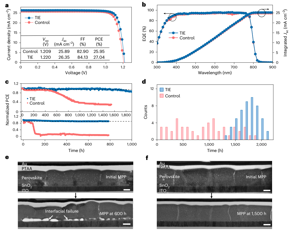
(a) J–V curves and photovoltaic parameters of champion PSCs under reverse scanning. (b) EQE and integrated current-density curves for control and TIE devices. (c) Operational stability measured by maximum power point (MPP) tracking under one-sun illumination in N₂ at room temperature (RT) and 85°C. Initial PCE values for control and TIE devices in (c) were 22.82% and 23.73%, respectively. (d) Histograms of T80 lifetime distributions for different PSCs (n = 50 for each group). (e) Cross-sectional TEM images of control devices before and after room-temperature MPP tracking. (f) Cross-sectional TEM images of TIE devices before and after MPP tracking.
Under reverse scanning, the champion TIE device reached 27.04% efficiency, with a certified value of 26.67%, compared with 25.95% for the control. Across 50 devices per condition, average efficiency increased from 25.25% to 26.29%, with negligible hysteresis between reverse and forward scans. The bandgap derived from the derivative of the external quantum efficiency spectrum was 1.55 eV, corresponding to an open-circuit voltage deficit as low as 0.33 V. EQE-integrated current densities were 25.41 mA cm⁻² for TIE and 24.88 mA cm⁻² for the control, consistent with values extracted from the J–V curves. Improved quantum efficiency in the 650–780 nm and 350–500 nm ranges was attributed to optimized energy-level alignment at the device heterointerface. Only trace AIBN remained after processing, with negligible impact on device performance. TIE was also applicable to p–i–n architectures.
The stability differences were primarily associated with mechanical failure. Under ISOS-L-1, the control devices began at 22.82% efficiency, remained stable for the first 400 h, and then exhibited a sharp decline between 400 and 600 h. TIE devices retained 95% of their initial efficiency (23.73%) after 1,500 h of operation. The control T80 lifetimes ranged from tens of hours to more than 1,800 h, while TIE lifetimes clustered near 1,800 h; 92% of TIE devices reached a T80 lifetime of 1,400 h. Under ISOS-L-2 at 85°C, all four TIE devices retained more than 90% of their initial efficiency (approximately 23%) after 800 h, whereas control devices often failed catastrophically within 200 h. Cross-sectional TEM localized failure in control devices to the perovskite/ETL heterointerface, which remained intact in TIE devices. After 300 thermal cycles, TIE devices exhibited almost no efficiency loss, while control devices retained 84%. In damp-heat tests, TIE devices retained 90% of their initial efficiency after 1,000 h, versus less than 50% for the control.
TIE uses a covalently bonded trans-interface polymer network to achieve two objectives simultaneously: mechanically integrating the perovskite and electron transport layers, and passivating interfacial defects. Improved charge extraction accounts for the efficiency gain, while reduced mechanical failure during operation explains the stability improvement and narrower device-to-device T80 distribution. The authors note that the radical-derived copolymer network may itself undergo long-term aging. Although the proof-of-concept devices have passed multiple accelerated-aging protocols, future work will focus on intrinsically more stable monomers and controlled in-situ polymerization within device architectures.
It creates covalently bonded polymer nano-linkages across the perovskite/SnO₂ interface, improving mechanical adhesion and reducing interfacial defects and delamination.
Q2: What efficiency did the TIE devices achieve?The champion device achieved 27.04% power conversion efficiency, with a certified efficiency of 26.67%. The average efficiency of 50 devices increased from 25.25% to 26.29%.
Q3: What did the T80 lifetime tests show?Under ISOS-L-1 maximum power point tracking, 92% of TIE devices reached a T80 lifetime of 1,400 hours. TIE devices also retained 95% of their initial efficiency after 1,500 hours.
E-mail: market@millennialsolar.com
The Millennial Solar perovskite MPPT testing system uses a Class 3A+ LED solar simulator as an aging light source. Compared with the previous generation, the spectral range has been extended to 300–1700 nm (AM0), the spectral classification reaches AAA (AM0), and 24 channels can be adjusted independently. The system supports research on perovskite solar cells, space photovoltaics, and tandem cells (2T/3T/4T).
▶ Light source classification: AAA (AM0), with a spectral range of 300–1700 nm for space photovoltaic testing.
▶ Independent multi-band control: 24 adjustable channels (AM0) for matching the subcell bandgaps of triple- and quadruple-junction tandem cells.
▶ Large-area sample fixture: Supports tandem cells up to 210 × 105 mm, using front- and rear-side gold-wire pressure contacts for electrode connection.
▶ Environmental control: Semiconductor-based temperature control from 15°C to 100°C, with testing available in a moisture- and oxygen-free nitrogen atmosphere.
The Millennial Solar perovskite MPPT testing system serves not only as a performance verification tool but also as an efficient testing platform for research on perovskite and tandem solar cells.
Original Research Reference: Trans-interface engineering for reliable perovskite solar cells with reproducible stability
*Disclaimer: Original and reproduced articles published by this account are intended solely for academic sharing and the dissemination of industry information. Unauthorized plagiarism, alteration, quotation, or republication that infringes upon the rights of this account is prohibited. The content is for reference only. If there are copyright concerns, please contact our company for removal.
Related Products


