


Non-contact IV tester

Quantum Efficiency Tester
PL/EL Integrated System
PV-Reflectumeter
3D Confocal Microscope
In-Line Four Point Probe Tester
Four Point Probe Tester
In-Line Thin Film Thickness Tester
Raman Spectrometer
FTIR Spectrometer
Spectrophotometer
Automatic Spectroscopic Ellipsometer
Contact Resistance Tester
Ultra depth of field 3D microscope
Auto Visual Tester
VMM PV Vision Measuring Machine
Solar Cell Horizontal Tensile Tester
Steady State Solar Simulator for Solar Cell
Solar Cell UV Aging Test Chamber
Solar Cell Comprehensive Tensile Tester
Visual Inspection Tester
Wet Leakage Current Tester
PV Module EL Tester
PV Module UV Preconditioning Chamber
Steady State Solar Simulator for PV Module
Current Continuous Monitor
Potential Induced Degradation Test
Bypass Diode Tester
LeTID Test System
Reverse Current Overload Tester
Impulse Voltage Tester
Hipot Insulation Tester
Ground Continuity Tester
Hipot Insulation Ground Tester
Damp Heat Test Chamber
Humidity Freeze Test
Thermal Cycle Test Chamber
Dynamic Mechanical Load Tester
Static Mechanical Load Tester
Hail Impact Tester
Robustness of Termination Tester
Module Breakage Tester
Cut Susceptibility Tester
Peel Shear Strength Tester
Universal Testing Machine (Single-arm)
Universal Testing Machine (Double-arm)
Glass Transmittance Tester
Acetic Acid Test Chamber
EVA Degree of Crosslinking Test System
Junction Box Comprehensive Tester
Drop ball tester
Semi-automatic scanning four-probe tester
Stylus Profilometer
Maximum Power Point Tracker
Perovskite Glass Transmittance Tester
Perovskite P1 Laser Scribing Multifunctional Testing Machine
Perovskite Online PL Tester
Perovskite Online Sheet Resistance Tester
Online Perovskite Film Thickness Tester
Perovskite Process Inspection Workstation
Portable EL Tester
Portable Thermal Imaging Tester
Solar Module Multi-Channel Testing System
PV Inverter Power Quality Tester
IV Tester
IVEL Cell Sorting Machine
BC Cell Grid Line Optimization and Inspection: Analysis of the ZBB Silver-Saving Solution Without Main Grids
Date : 15 September 2026Views : 30
Back-contact (BC) cells relocate both the positive and negative electrodes to the rear side,leaving the front completely free of metal gridlines. This reduces shading losses to zero, benefiting both efficiency and aesthetics.TOPCon back-contact (TBC), heterojunction back-contact (HBC), and hybrid passivated back-contact (HPBC) all follow this approach; the only difference lies in the passivation and doping patterns on the back side. The trade-off shifts to the same side: p-type and n-type patterns are crowded together, limiting design flexibility and complicating the process. Fortunately, processes such as laser film removal, laser-enhanced contact optimization (LECO), and thermal laser separation have gradually matured, driving down mass production costs and allowing the market share of back-contact (BC) cells to begin climbing. The Millennial Solar TLM contact resistance tester is a high-precision analytical instrument specifically designed to extract key electrical parameters for solar cell electrode optimization, featuring dual testing capabilities for contact resistivity and line resistance.
TOPCon and SHJ technologies already consume more silver paste than PERC, and with silver prices remaining high, “using less silver without sacrificing efficiency” has become a pressing need. The grid line layout directly determines silver paste consumption, leading to the emergence of the zero-busbar (ZBB) structure: the pads and main busbars are removed, and the interconnect ribbons are directly bonded onto the fine grid lines.The loss profiles and optimal parameters differ between these two designs. The following section first outlines the models and settings, then discusses the results separately, and finally compares them in a single efficiency–silver paste plot.
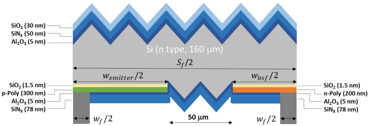
Schematic cross-section of a c-Si TBC solar cell in the thickness direction (not to scale)
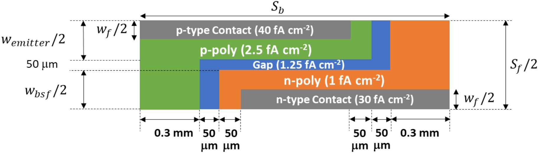
Quokka3 modeling using quarter-cell fine-grid geometry (showing the back side of the TBC solar cell)
The methodology is divided into three layers, each addressing a specific physical aspect. For the optical analysis, the ray-tracing software SunSolve Power is used to account for light trapping in the textured surface; for the electrical analysis, Quokka3 is used, treating the heavily doped poly thin layer as a conductive boundary layer and modeling it using two lumped parameters—saturation current density and sheet resistance. Losses in the metal grid lines are calculated separately using analytical equations: geometric parameters such as the main grid width, thickness, and the size and number of pads are converted into metal resistance power losses, saving time that would otherwise be spent modeling each grid line individually. The cell efficiency is obtained by subtracting these metal losses from the electrical results generated by Quokka; silver paste consumption is converted into the mass of silver paste (mg/W) corresponding to the output per watt under AM1.5G conditions.
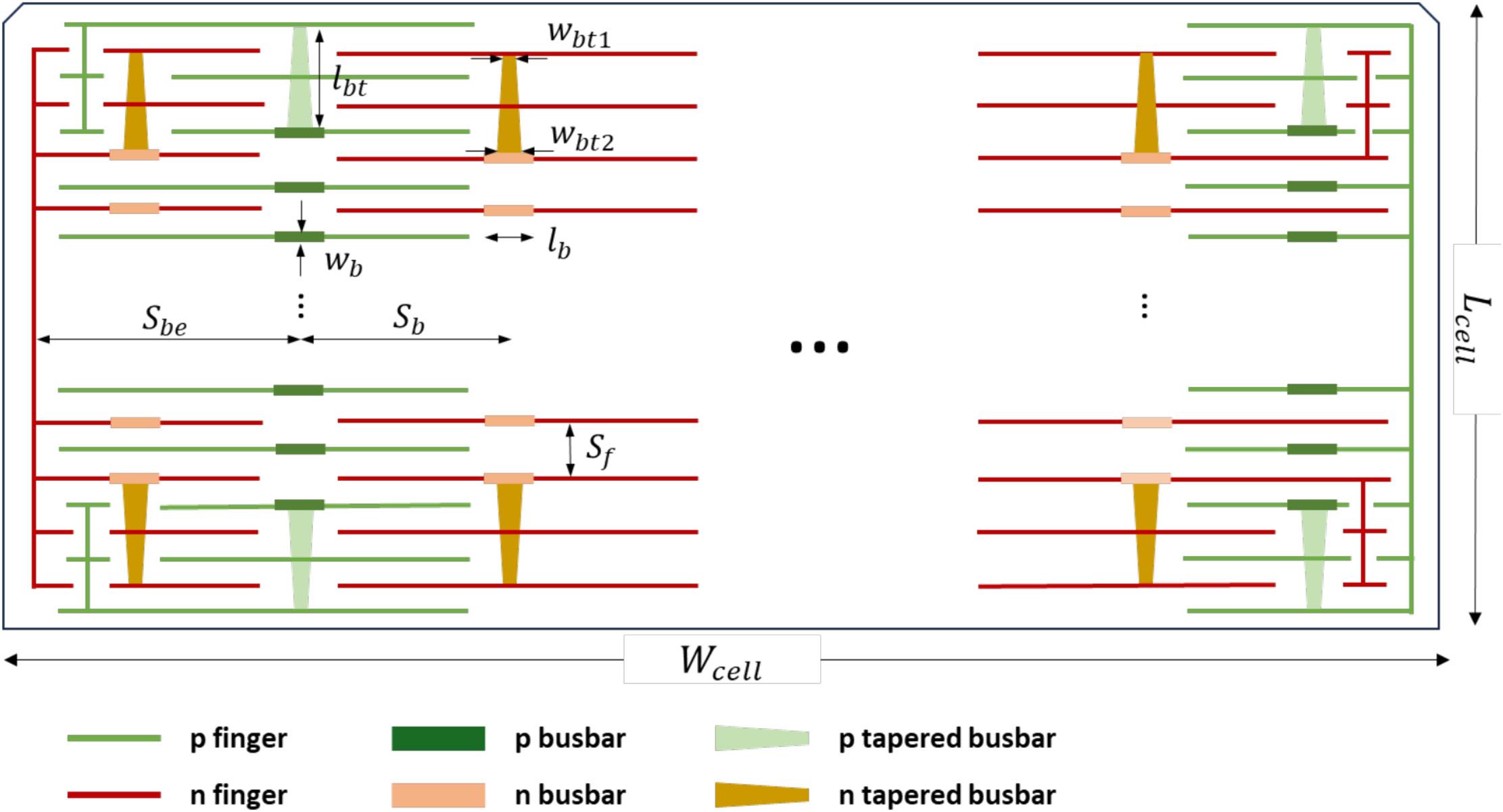
Schematic of grid line geometry for a zero-back-bus (ZBB) TBC solar cell (not to scale)
The simulation model is a G12R half-cell TBC cell, 182 × 105 mm and 160 μm thick.The front surface features a random pyramid texture with a base angle of 53°, overlaid with an Al₂O₃/SiNX/SiO₂anti-reflection stack; the back surface is divided into three regions: p-poly, n-poly, and an undoped gap, with the two poly regions maintained as flat surfaces to facilitate passivation. Electrical parameters were obtained from symmetric samples provided by an industry partner and measured using the transmission line method. Grid lines were systematically scanned for fine grid spacing (Sf) of 0.8–1.3 mm, fine grid width (wf) of 20–35 μm, and the number of main grids (Nb) ranging from 20 to 30.In the pad-type layout, the first and last main gates are positioned close to the cell edges, and the pads are shifted inward toward the center to ensure reliable string bonding; the spacing is set to 1.5 times the conventional value.
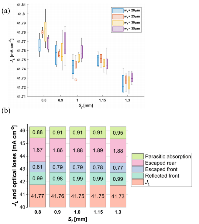
(a) Simulated photogenerated current density JL of a 160 μm-thick TBC cell as a function of fine-grid spacing Sf and fine-grid width wf; (b) Breakdown of optical losses obtained from SunSolve simulations
In the optical simulation, the photogenerated current density JL is first set to a baseline value. As the fine-grid spacing increases, the proportion of the back-surface area rises, leading to poorer light trapping and increased light escape, causing JL to decline; the fine-grid width, however, has almost no effect on JL, as very little light falls on the fine grids to begin with, and approximately 80% of that is lost through diffuse reflection.When breaking down the losses item by item, rear-surface escape is the largest single component, followed by front-surface reflection; neither of these changes with fine-grid spacing. Parasitic absorption becomes more significant as the spacing increases.The simulated JL was slightly lower than expected overall, which the authors attributed to three factors: the front surface texturing was not optimized for the BC junction, the ARC stack was simplified, and the model treated the back surface as air, whereas the test setup actually used a reflective substrate. These discrepancies only affect absolute values and do not alter the relative ranking of the grating lines.
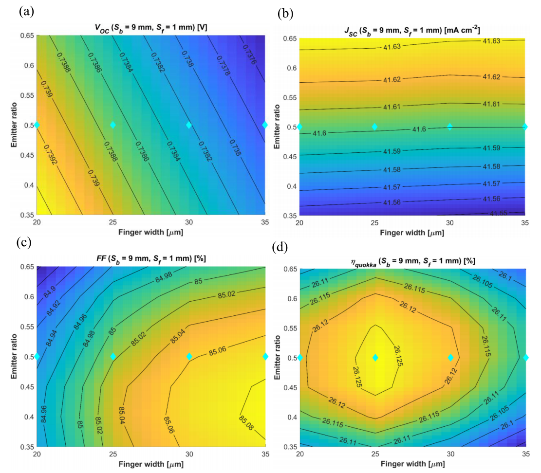
(a) VOC, (b) JSC, (c) FF, and (d) ηquokka obtained from Quokka3 simulations
The electrical simulation begins with the emitter ratio. This ratio is equal to the emitter width divided by the fine-gate pitch; it relates to both electrical shielding and surface recombination and carrier transport. Since the saturation current density and sheet resistance of p-poly are both higher than those of n-poly, the value naturally requires a compromise.Across the entire range of fine-gate widths from 20 to 35 μm, the optimal ratio remained at 0.5. Lowering the ratio and narrowing the fine gate benefits VOC; increasing the ratio reduces transport losses of minority carriers in the BSF region, benefiting JSC; FF, however, peaks at a certain ratio in the middle range.
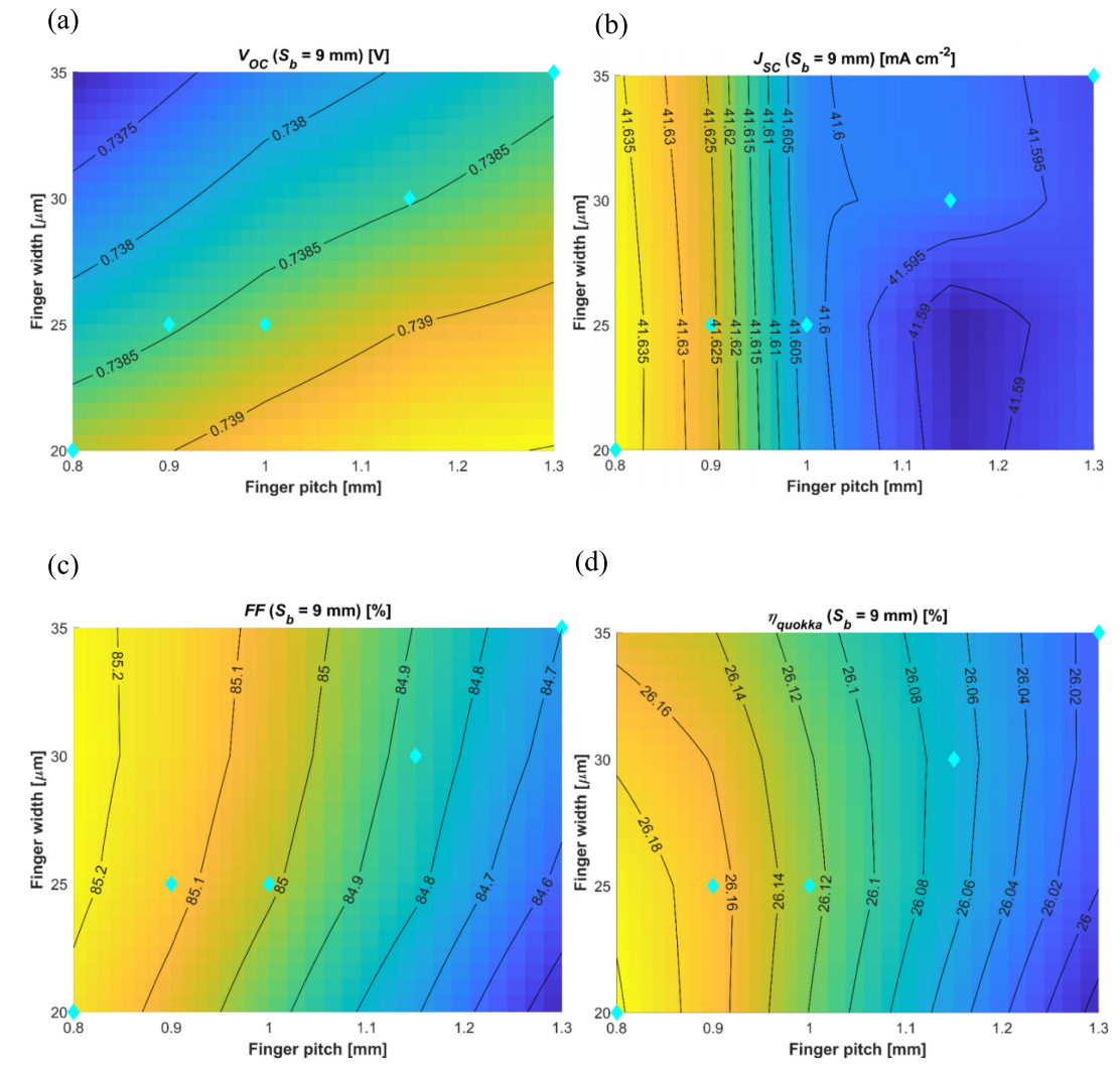
(a) VOC, (b) JSC, (c) FF, and (d) ηquokka obtained from Quokka3 simulations
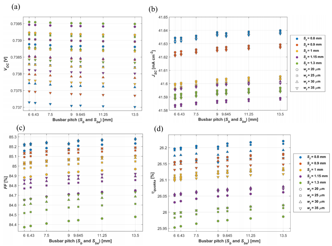
(a) VOC, (b) JSC, (c) FF, and (d) ηquokka obtained from Quokka3 simulations
When all five fine-gate spacings, four widths, and seven main-gate spacings are laid out, only two patterns remain: the smaller the spacing, the higher ηquokka; the larger the spacing, the wider the optimal fine-gate width. The level of VOC is determined by the ratio of fine-gate width to spacing, while the combined weight of FF and JSC outweighs that of VOC.
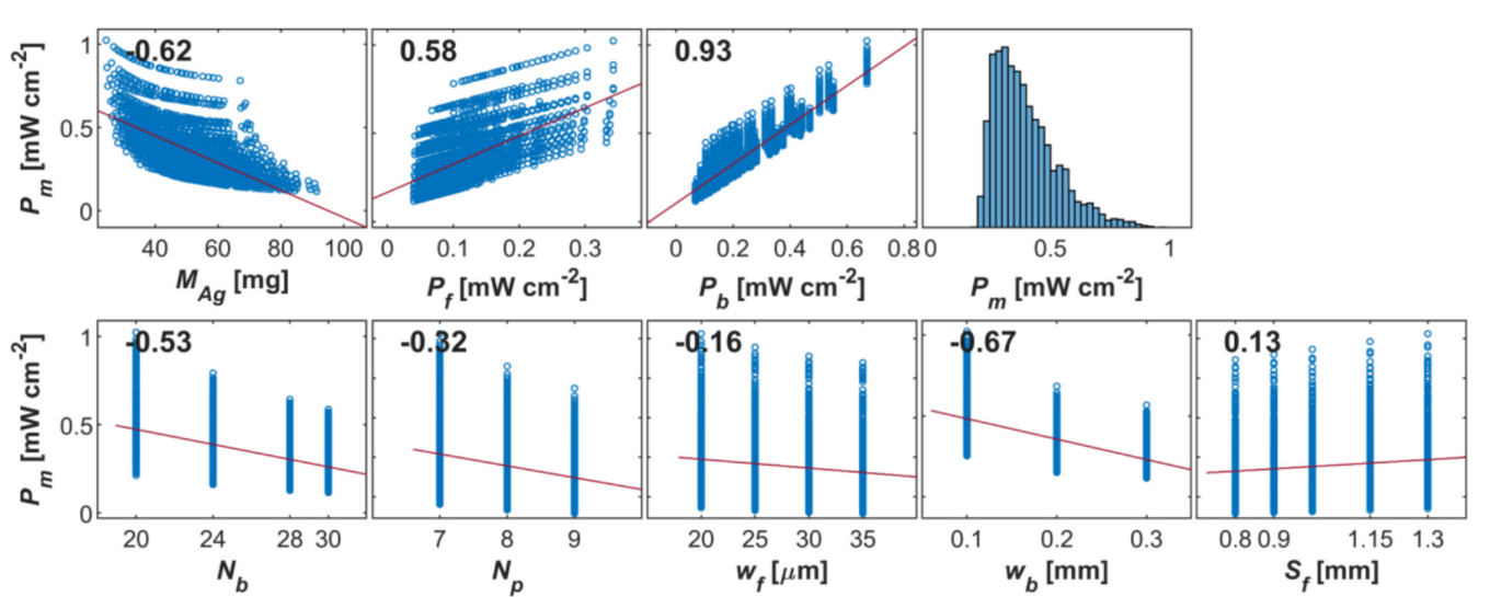
Correlation matrix of power loss due to metal resistance in pad-type TBC cells versus various parameters
In pad-type designs, the correlation coefficient between main grid losses and total metal losses is as high as 0.93, while that for fine grid losses is only 0.58, indicating that the main grid accounts for the lion’s share of losses.Widening the main grid, increasing the grid density, and adding more pads all yield immediate results, with corresponding correlation coefficients of −0.67, −0.53, and −0.32, respectively—significantly stronger than the parameters related to the fine grid.
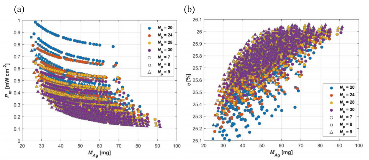
Scatter plots of (a) Pm and (b) η for pad-type TBC cells as a function of the number of main grids (Nb) and the number of pads (Np)
In terms of numbers, the efficiencies for Nb = 28 and 30 are nearly identical; adding more main gates offers limited benefit, and the resistance of the solder bands at the module level warrants further investigation; the electrical shading caused by increased pad area is another cost that must be closely monitored.
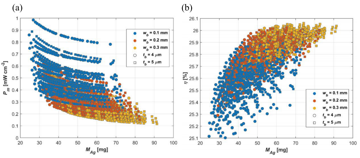
Scatter plots of (a) Pm and (b) η for pad-type TBC cells as a function of main grid width wb and main grid thickness tb
The optimal value for the main grid width depends on the silver paste budget: when silver paste is abundant (>50 mg), use 0.3 mm; when the budget is tightened to below 40 mg, switch to 0.1 mm, and allocate the saved silver paste to a smaller fine-grid pitch.
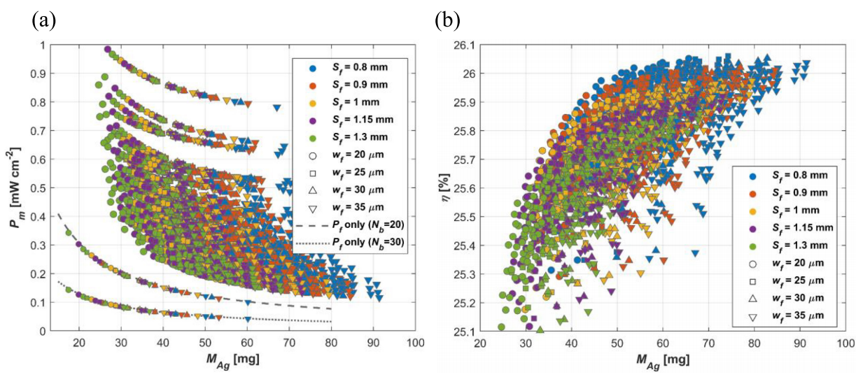
Scatter plots of (a) Pm and (b) η as functions of fine-grid spacing Sf and fine-grid width wf for pad-type TBC cells
The most efficient combination generally occurs at Sf = 0.8 mm and wf = 20 μm; only when the budget falls below 40 mg do larger spacing values outperform this combination. Pure fine-grid losses are significantly lower than the total losses including the main grid; therefore, eliminating the main grid is the primary strategy for saving silver.
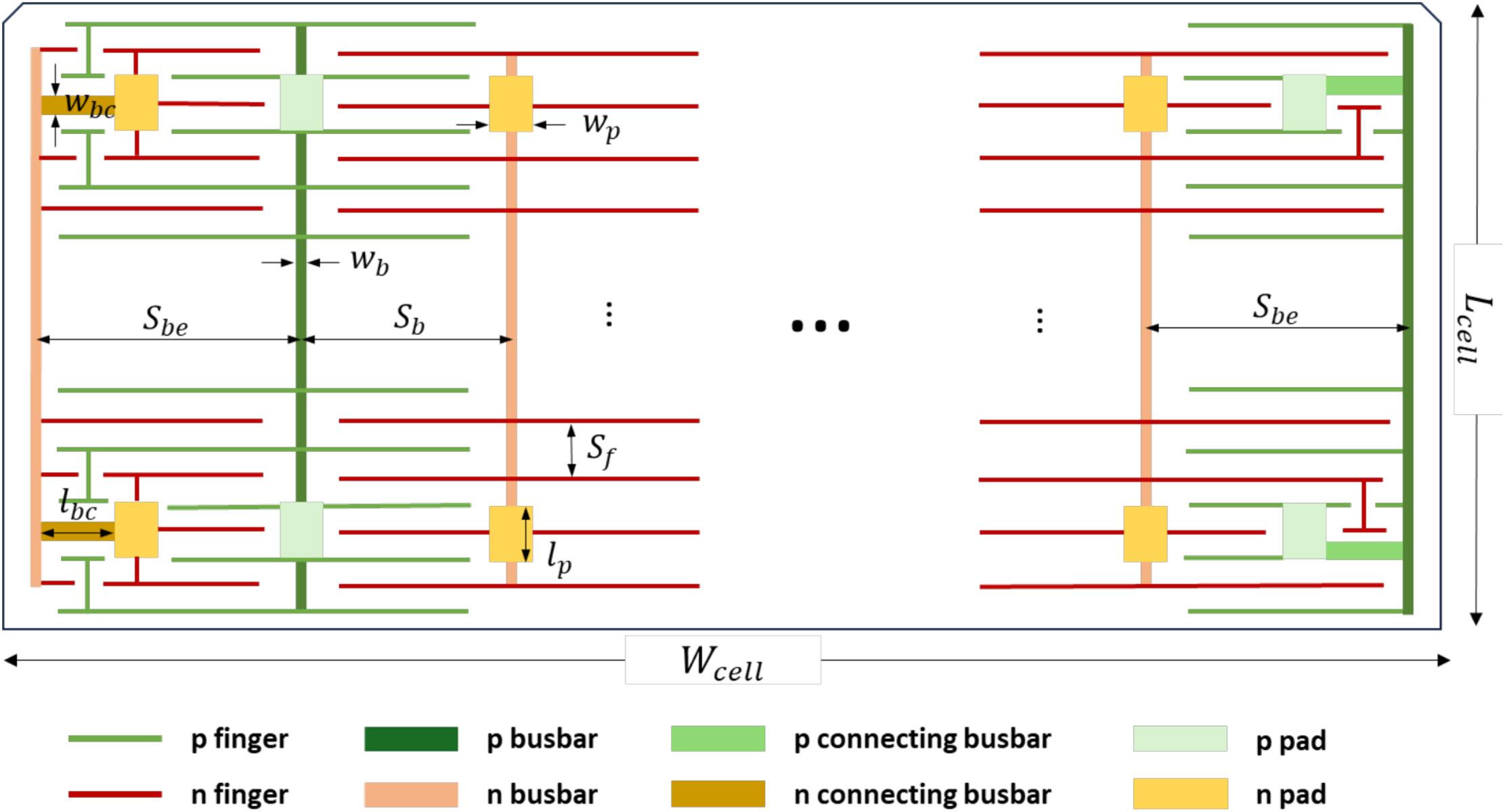
Schematic of grid line geometry for pad-type TBC solar cells (not to scale)
With ZBB, the situation is reversed. The bond wire is electrically connected to each fine grid, causing the correlation coefficient between fine grid losses and total losses to rise to 0.96, with a quadratic dependence on fine grid length.In this scenario, the number of main busbars remains the most critical parameter: Nb = 30 yields both the lowest loss and the highest efficiency, with Nb = 28 following closely behind; conversely, the main busbar width becomes the parameter with the weakest correlation, and its optimal value becomes more flexible as the silver paste budget increases.
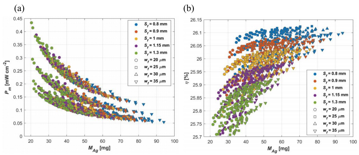
Scatter plots of (a) Pm and (b) η for ZBB TBC cells as a function of fine-grid spacing Sf and fine-grid width wf
The originally continuous main grid has been degraded into short, segmented lines parallel to the fine grids, with a conical main grid added to collect current from the edge fine grids.The conclusions regarding the fine grid side are consistent with those for the pad-type design: at Sf = 0.8 mm, the ηquokka advantage is solid; when the silver paste budget is below 50 mg, wf is set to 20 μm, and when the budget is ample, it can be relaxed to 35 μm.
Trade-offs Between the Two Designs
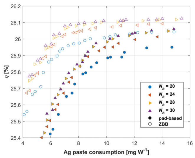
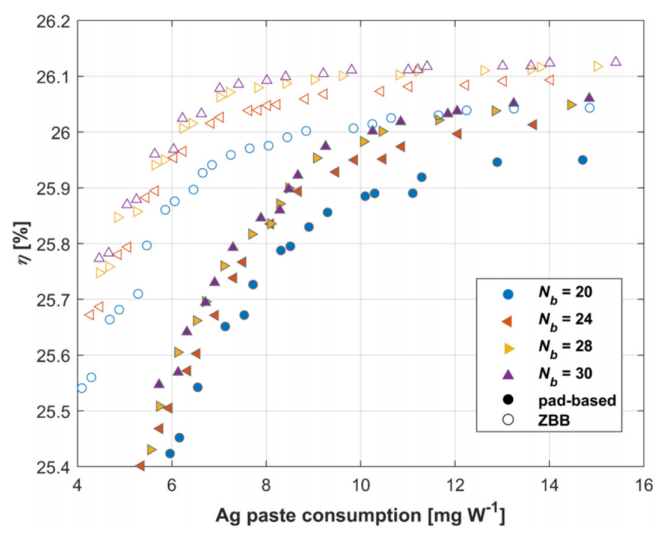
Contour lines of maximum efficiency η for pad-type (solid symbols) and ZBB (hollow symbols) TBC cells versus silver paste consumption and number of main busbars Nb
When the efficiency versus silver paste consumption curves for both designs are plotted on the same graph, the difference is immediately apparent. For the pad-type design to maintain an efficiency of 26% ± 0.1%, silver paste consumption must not fall below 11 mg/W; the ZBB design requires only about 7 mg/W. At the same silver paste consumption, the ZBB design’s efficiency is 0.1 ± 0.02 percentage points higher (in absolute terms);When the budget is reduced to below 10 mg/W, the gap widens significantly. By comparison, reducing the number of main gates from 30 to 20 results in a loss of approximately 0.1 percentage points for both designs. In terms of silver savings, ZBB is the clear winner; however, this comes at a cost elsewhere: higher thresholds for interconnection processes and module reliability, requiring item-by-item verification prior to mass production.
This paper employs SunSolve for optical simulation, Quokka3 for electrical simulation, and analytical calculations to account for metal resistance losses, conducting a systematic grid line optimization for c-Si TBC cells with both pad-type and ZBB designs.Optical simulations show that cell JSC is independent of fine-line width and decreases only slightly as fine-line spacing increases. After importing the simulated current generation rates into the Quokka electrical model, the optimal emitter width was first determined for each fine-line configuration. The simulation was then extended to all possible main-line spacings, and finally, the Quokka simulation results were combined with analytically calculated metal power losses to determine cell efficiency.
Frequently Asked Questions (FAQ)
Q1: Why does the ZBB design save more silver than the pad-type design?
In pad-type designs, the main busbar accounts for the lion's share of metal losses, with a correlation coefficient as high as 0.93. ZBB removes the pads and main busbars entirely, bonding interconnect ribbons directly onto the fine grid lines. As a result, ZBB maintains 26% efficiency with only about 7 mg/W of silver paste, while the pad-type design requires at least 11 mg/W—and at the same silver consumption, ZBB delivers 0.1 ± 0.02 percentage points higher efficiency.
Q2: What are the optimal fine-grid parameters for TBC cells?
Across fine-grid widths from 20 to 35 μm, the optimal emitter ratio stays at 0.5. The most efficient combination occurs at a fine-grid spacing Sf = 0.8 mm and width wf = 20 μm. When the silver paste budget is ample (above 50 mg), wf can be relaxed to 35 μm; when the budget is tight, smaller spacing and narrower fingers should be prioritized.
Q3: What is the most critical control parameter in the ZBB design?
With ZBB, fine-grid losses dominate (correlation coefficient 0.96), but the number of busbars remains the key control parameter: Nb = 30 yields both the lowest loss and the highest efficiency, with Nb = 28 close behind.
Millennial Solar TLM Contact Resistance Tester
email:market@millennialsolar.com
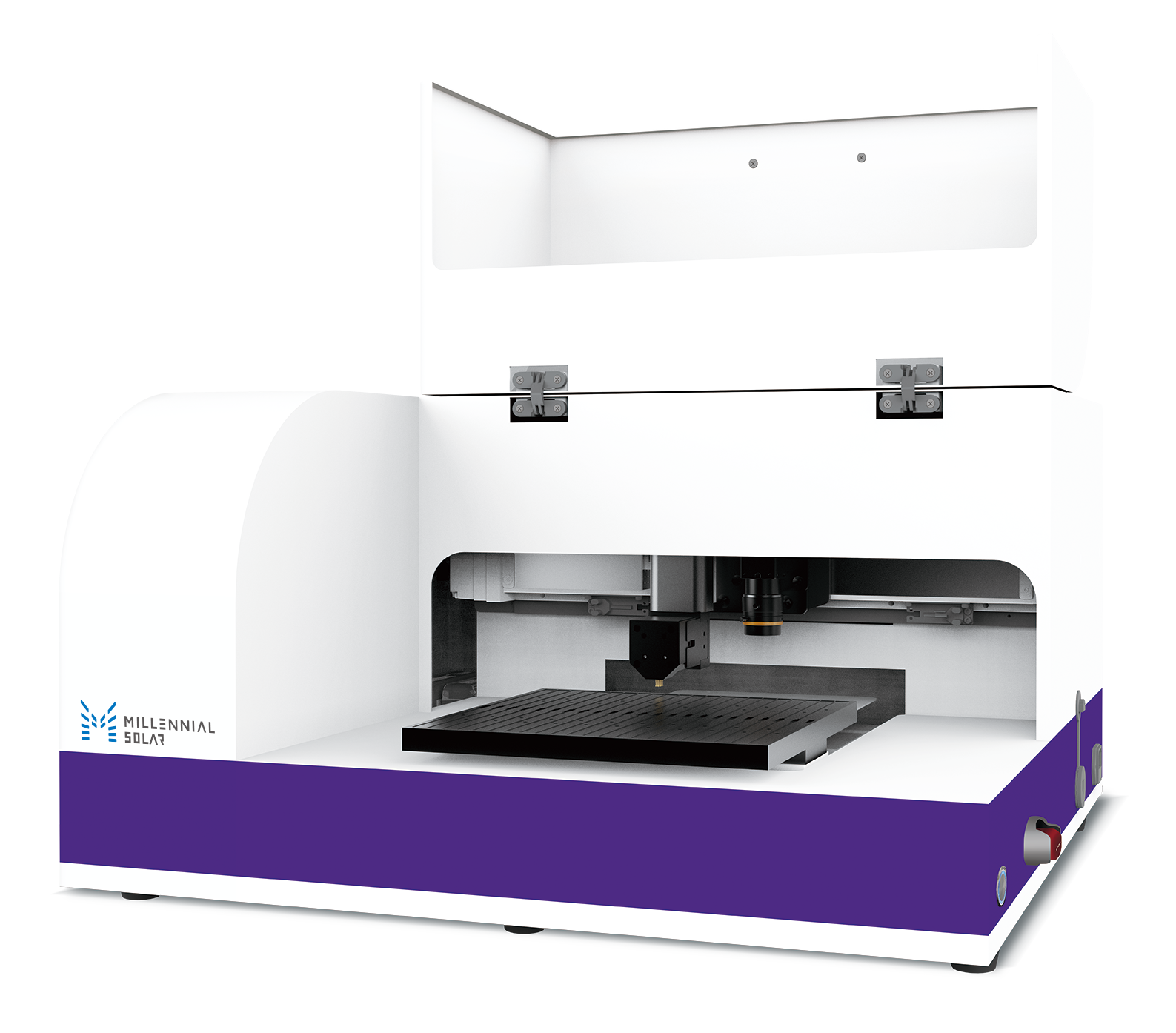
The Meineng TLM Contact Resistance Tester features contact resistivity testing capabilities, enabling fast, flexible, and accurate testing.
Static test repeatability ≤ 1%; dynamic test repeatability ≤ 3%
● Wire resistance measurement accuracy up to 5% or 0.1 Ω/cm
● Seamless switching between contact resistivity and line resistance testing
● Customizable probes for measurement and analysis
Related Products


