
Quantum Efficiency Tester
PL/EL Integrated System
PV-Reflectumeter
3D Confocal Microscope
In-Line Four Point Probe Tester
Four Point Probe Tester
In-Line Thin Film Thickness Tester
Raman Spectrometer
FTIR Spectrometer
Spectrophotometer
Automatic Spectroscopic Ellipsometer
Contact Resistance Tester
Ultra depth of field 3D microscope
Auto Visual Tester
VMM PV Vision Measuring Machine
Solar Cell Horizontal Tensile Tester
Steady State Solar Simulator for Solar Cell
Solar Cell UV Aging Test Chamber
Solar Cell Comprehensive Tensile Tester
Visual Inspection Tester
Wet Leakage Current Tester
PV Module EL Tester
PV Module UV Preconditioning Chamber
Steady State Solar Simulator for PV Module
Current Continuous Monitor
Potential Induced Degradation Test
Bypass Diode Tester
LeTID Test System
Reverse Current Overload Tester
Impulse Voltage Tester
Hipot Insulation Tester
Ground Continuity Tester
Hipot Insulation Ground Tester
Damp Heat Test Chamber
Humidity Freeze Test
Thermal Cycle Test Chamber
Dynamic Mechanical Load Tester
Static Mechanical Load Tester
Hail Impact Tester
Robustness of Termination Tester
Module Breakage Tester
Cut Susceptibility Tester
Peel Shear Strength Tester
Universal Testing Machine (Single-arm)
Universal Testing Machine (Double-arm)
Glass Transmittance Tester
Acetic Acid Test Chamber
EVA Degree of Crosslinking Test System
Junction Box Comprehensive Tester
Drop ball tester
Semi-automatic scanning four-probe tester
Stylus Profilometer
Maximum Power Point Tracker
Perovskite Glass Transmittance Tester
Perovskite P1 Laser Scribing Multifunctional Testing Machine
Perovskite Online PL Tester
Perovskite Online Sheet Resistance Tester
Online Perovskite Film Thickness Tester
Perovskite Process Inspection Workstation
Portable EL Tester
Portable Thermal Imaging Tester
Solar Module Multi-Channel Testing System
PV Inverter Power Quality Tester
Drone EL Tester
IV Tester
IVEL Cell Sorting Machine
An Important Process in the Production of Solar Cells - Screen Printing
Date : 27 September 2023Views : 1935
In the manufacturing process of solar cells, in order to prepare solar cell contact electrodes, it is necessary to print metal paste on silicon wafers by screen printing technology. After the sintering process, front and back electrodes are formed on the surface of the solar cell, through which the current of the cell is collected and transmitted.Millennial 3D microscope can detect the number of grid lines and pyramids on the photovoltaic cell through the system software, helping users to master the quality of solar cell cleaning, texturing, and screen printing processes.
![]()
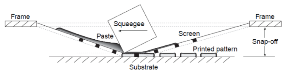
Screen Printing Process
The process steps of screen printing are: printing the back electrode with silver paste→drying→printing the back field with aluminum paste→drying→printing the front grid with silver paste→drying. The printed pattern is required to be complete, clear, uniform and symmetrical.
When performing screen printing, the printing pattern should be designed first and made into a screen. The meshes that need to form the graphics part on the screen are transparent, and the non-graphics parts are closed. When printing, spread the slurry on the screen, the blade of the scraper is close to the screen surface of the screen to scrape the slurry horizontally, and apply appropriate pressure to make the screen contact with the silicon wafer, and the slurry is squeezed out of the mesh and then adhered on a silicon wafer. Because there is a gap between the stencil and the silicon wafer, the stencil will use its own tension to contact the silicon wafer for an instant and then immediately break away from the silicon wafer and rebound. Graphically defined areas of the board are adhered to the slurry.
Using screen printing to make solar cell electrodes has the characteristics of low production cost and high production capacity, and is currently a widely used method in large-scale production. In addition to screen printing, there are other methods to make electrodes, such as groove buried grid method, inkjet printing method, stencil printing method, etc., but most of them have not been applied to large-scale production because of high cost or immature technology.
![]()
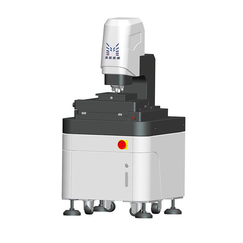
Millennial 3D Microscope
E-mail: market@millennialsolar.cn
Millennial 3D Microscope is a high-speed confocal scanning microscope for accurate and reliable 3-dimensional (3D) measurements. Real-time confocal microscopy images are realized by fast optical scanning modules and signal processing algorithms.
Millennial 3D Microscope has high-definition confocal microscopy technology, precise high-resolution scanning technology, and solvent materials that are difficult to distinguish on the surface can also be presented. The Z-axis display resolution is as high as 1nm, which can accurately obtain tiny shapes.
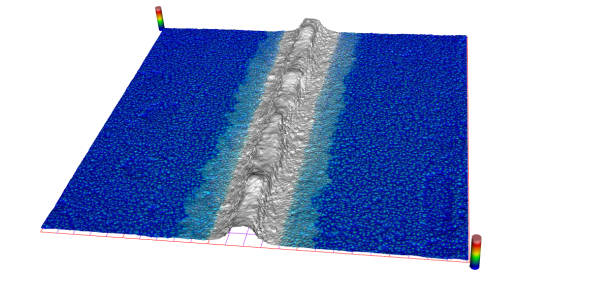
Based on the principle of optical technology, combined with precise Z-direction scanning module and 3D modeling algorithm, etc., non-contact scanning is performed on the surface of the device and a 3D image of the surface is established. Quantitative detection of the number of pyramids in order to feedback the quality of photovoltaic cell cleaning, texturing, and screen printing processes.


