
Quantum Efficiency Tester
PL/EL Integrated System
PV-Reflectumeter
3D Confocal Microscope
In-Line Four Point Probe Tester
Four Point Probe Tester
In-Line Thin Film Thickness Tester
Raman Spectrometer
FTIR Spectrometer
Spectrophotometer
Automatic Spectroscopic Ellipsometer
Contact Resistance Tester
Ultra depth of field 3D microscope
Auto Visual Tester
VMM PV Vision Measuring Machine
Solar Cell Horizontal Tensile Tester
Steady State Solar Simulator for Solar Cell
Solar Cell UV Aging Test Chamber
Solar Cell Comprehensive Tensile Tester
Visual Inspection Tester
Wet Leakage Current Tester
PV Module EL Tester
PV Module UV Preconditioning Chamber
Steady State Solar Simulator for PV Module
Current Continuous Monitor
Potential Induced Degradation Test
Bypass Diode Tester
LeTID Test System
Reverse Current Overload Tester
Impulse Voltage Tester
Hipot Insulation Tester
Ground Continuity Tester
Hipot Insulation Ground Tester
Damp Heat Test Chamber
Humidity Freeze Test
Thermal Cycle Test Chamber
Dynamic Mechanical Load Tester
Static Mechanical Load Tester
Hail Impact Tester
Robustness of Termination Tester
Module Breakage Tester
Cut Susceptibility Tester
Peel Shear Strength Tester
Universal Testing Machine (Single-arm)
Universal Testing Machine (Double-arm)
Glass Transmittance Tester
Acetic Acid Test Chamber
EVA Degree of Crosslinking Test System
Junction Box Comprehensive Tester
Drop ball tester
Semi-automatic scanning four-probe tester
Stylus Profilometer
Maximum Power Point Tracker
Perovskite Glass Transmittance Tester
Perovskite P1 Laser Scribing Multifunctional Testing Machine
Perovskite Online PL Tester
Perovskite Online Sheet Resistance Tester
Online Perovskite Film Thickness Tester
Perovskite Process Inspection Workstation
Portable EL Tester
Portable Thermal Imaging Tester
Solar Module Multi-Channel Testing System
PV Inverter Power Quality Tester
Drone EL Tester
IV Tester
IVEL Cell Sorting Machine
An Important Preparation Process for Depositing ITO Thin Films - PECVD Coating
Date : 17 October 2023Views : 1555
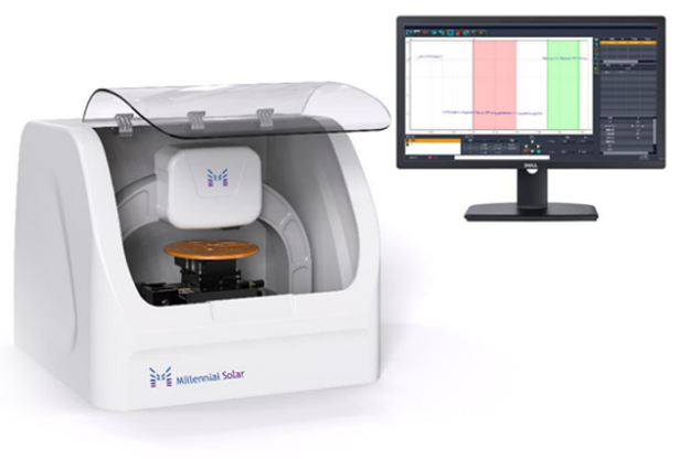
As a process in solar cell production, PECVD plays a key role in improving its performance. PECVD can deposit silicon nitride thin films on the surface of solar cells, thereby effectively improving the photoelectric conversion rate of solar cells. However, in order to clearly and objectively detect the ITO film of the solar cell after deposition and understand various parameters such as the film thickness and surface roughness, Stylus Profiler must be used for measurement. The Stylus Profiler produced by "Millennial Solar" can measure various parameter information such as surface roughness and warping stress of silicon nitride films in solar cells, and evaluate issues related to solar cell performance for photovoltaic enterprise users.
![]()
In-depth understanding of the basic principles of PECVD process
PECVD, also called plasma chemical vapor deposition, is a thin film growth technology that uses plasma to deposit at low temperatures.PECVD technology uses low-temperature plasma to generate glow discharge on the cathode of the process chamber under low pressure, and then uses the glow discharge to heat the sample to a predetermined temperature.Then an appropriate amount of process gas is introduced, and these gases are decomposed at high temperature through a series of chemical reactions and plasma reactions to generate the required compounds, and then the compounds are deposited on the surface of the solar cell or other substrate materials to form a thin film.
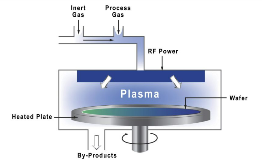
Basic principles of PECVD process
![]()
Process advantages of PECVD
Compared with traditional CVD, one of the main advantages of PECVD is that it can operate at lower temperatures, thereby reducing thermal stress on the substrate material, and is widely applicable to the manufacturing of solar cells. The PECVD plasma contains a large number of high-energy electrons, which can provide the activation energy required for the chemical vapor deposition process.The collision of electrons and gas phase molecules can promote the decomposition, combination, excitation and electrical processes of gas molecules, generating various highly active chemical groups, thereby significantly reducing the temperature range of CVD film deposition, making it possible to perform processes that originally required high temperatures. Thin film deposition is also possible at low temperatures.
![]()
Millennial Stylus Profiler
E-mail: market@millennialsolar.cn
Millennial Stylus Profiler is an advanced micro-nano measuring instrument that uses excellent instrument system construction and optimized measurement and data processing software to measure surface roughness, waviness, surface 2D/3D shape, warpage and stress. This enables reliable, efficient, and simple sample testing and completes perfect control from research and development to quality control.
●Equipped with 5 million pixel high-resolution color camera
●Step height repeatability 1nm
●Ultra-high straightness guide rail, reflecting the micro-morphology of the sample
●Sub-angstrom resolution, up to 0.01 angstrom in 13μm range
●High and low noise ratio and low linear error
As a key step that can directly improve the performance of solar cells through thin film deposition, the PECVD process has always been a process that major photovoltaic cell manufacturers focus on. Stylus Profiler produced by "Millennial Solar" relies on unique detection technology to provide targeted detection of silicon nitride films deposited on the surface of solar cells, helping photovoltaic cell manufacturers evaluate the performance of solar cells after film deposition, thereby achieving strong scientific proof !


