
Quantum Efficiency Tester
PL/EL Integrated System
PV-Reflectumeter
3D Confocal Microscope
In-Line Four Point Probe Tester
Four Point Probe Tester
In-Line Thin Film Thickness Tester
Raman Spectrometer
FTIR Spectrometer
Spectrophotometer
Automatic Spectroscopic Ellipsometer
Contact Resistance Tester
Ultra depth of field 3D microscope
Auto Visual Tester
VMM PV Vision Measuring Machine
Solar Cell Horizontal Tensile Tester
Steady State Solar Simulator for Solar Cell
Solar Cell UV Aging Test Chamber
Solar Cell Comprehensive Tensile Tester
Visual Inspection Tester
Wet Leakage Current Tester
PV Module EL Tester
PV Module UV Preconditioning Chamber
Steady State Solar Simulator for PV Module
Current Continuous Monitor
Potential Induced Degradation Test
Bypass Diode Tester
LeTID Test System
Reverse Current Overload Tester
Impulse Voltage Tester
Hipot Insulation Tester
Ground Continuity Tester
Hipot Insulation Ground Tester
Damp Heat Test Chamber
Humidity Freeze Test
Thermal Cycle Test Chamber
Dynamic Mechanical Load Tester
Static Mechanical Load Tester
Hail Impact Tester
Robustness of Termination Tester
Module Breakage Tester
Cut Susceptibility Tester
Peel Shear Strength Tester
Universal Testing Machine (Single-arm)
Universal Testing Machine (Double-arm)
Glass Transmittance Tester
Acetic Acid Test Chamber
EVA Degree of Crosslinking Test System
Junction Box Comprehensive Tester
Drop ball tester
Semi-automatic scanning four-probe tester
Stylus Profilometer
Maximum Power Point Tracker
Perovskite Glass Transmittance Tester
Perovskite P1 Laser Scribing Multifunctional Testing Machine
Perovskite Online PL Tester
Perovskite Online Sheet Resistance Tester
Online Perovskite Film Thickness Tester
Perovskite Process Inspection Workstation
Portable EL Tester
Portable Thermal Imaging Tester
Solar Module Multi-Channel Testing System
PV Inverter Power Quality Tester
Drone EL Tester
IV Tester
IVEL Cell Sorting Machine
ITO Thin Film Deposition for Heterojunction Cells
Date : 27 October 2023Views : 1605
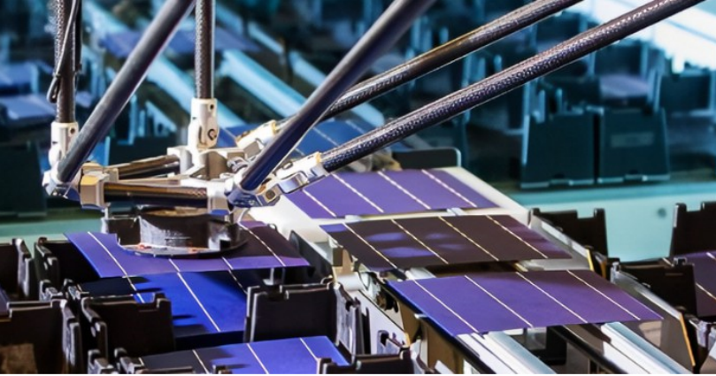
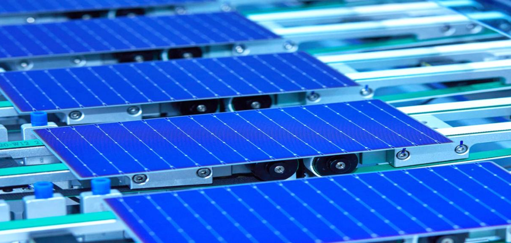
Since heterojunction cells are different from traditional thermal diffusion crystalline silicon solar cells, after completing the injection of the emitter and BSF, the next step is to deposit ITO films on the front and back of the heterojunction cell. The ITO film can compensate for the low conductivity of heterojunction cells after injecting the emitter. The Four-Point Probe Tester produced by Millennial Solar can efficiently measure the resistivity and sheet resistance of heterojunction cells after depositing ITO films, thereby evaluating whether the performance of heterojunction cells meets industrial standards.
![]()
Characteristics of ITO film
The ITO film is an N-type oxide semiconductor - indium tin oxide. Because it uses tin and oxygen as donors, it can maintain stable conductivity and visible light transmittance at room temperature. Due to its high mechanical hardness and good chemical stability, it can become a commonly used thin film material for heterojunction solar cells.
![]()
Problems with the process of preparing ITO thin films at low sputtering voltage
Since the ITO film itself contains oxygen, when the magnetron sputtering method is used to deposit the ITO film, a large number of oxygen anions will be generated. The oxygen anions will bombard the surface of the deposited ITO film with a certain particle energy under the action of the electric field. The crystal structure and crystal state of the ITO film cause structural defects. The greater the sputtering voltage, the greater the energy of oxygen negative ions bombarding the surface of the film layer. Therefore, the probability of causing such structural defects will increase, and the more serious the crystal structure defects will be, which causes the resistivity of the ITO film to increase.
Under normal circumstances, the sputtering voltage when depositing ITO films by magnetron sputtering is around -400V. If a certain process method is used to reduce the sputtering voltage by more than 50%, it will not only improve the quality of the ITO film, but also reduce the sputtering voltage by more than 50%. It can also reduce the resistivity of ITO film, also reduces the preparation cost of depositing ITO films into heterojunction cells.
![]()
Methods to reduce structural defects of ITO films
In order to reduce the sputtering voltage of the ITO film, it can be achieved by reasonably increasing the magnetic field intensity of the sputtering cathode. Therefore, a special set of sputtering cathode structure and sputtering DC power supply can be used. At the same time, the RF power supply can be reasonably installed on the DC power supply, and the process research on reducing the sputtering voltage of ITO thin films can be carried out under different DC sputtering power and RF power. , thereby effectively controlling the sputtering voltage when depositing the ITO film, and achieving the purpose of reducing the resistivity of the ITO film.
![]()
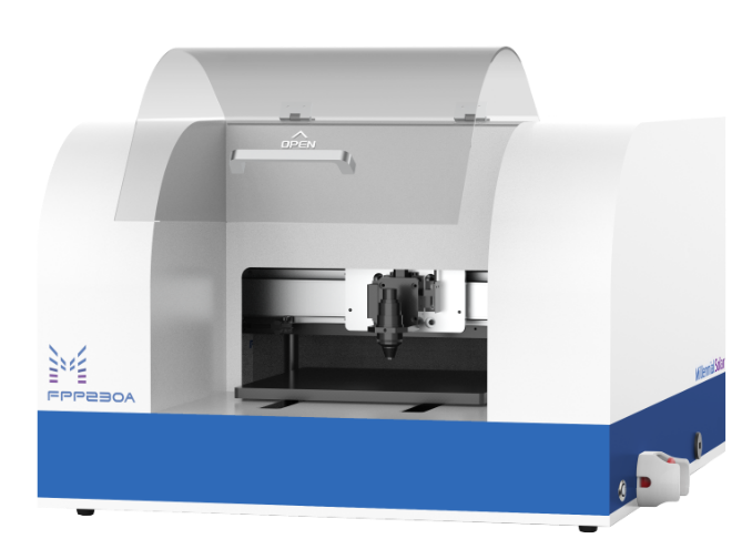
Four-Point Probe Tester
E-mail: market@millennialsolar.cn
Four-Point Probe Tester can quickly and automatically scan samples up to 230mm to obtain sheet resistance/resistivity distribution information at different locations of the sample. It can be widely used in photovoltaics, semiconductors, alloys, ceramics and many other fields.
● Ultra-high measurement range, measuring 0.1MΩ~100MΩ sheet resistance
● High-precision measurement, dynamic repetition rate can reach 0.2%
● Fully automatic multi-point scanning, multiple preset schemes can also be customized and adjusted
● Rapid material characterization and automatic calculation of correction factors
Since the low resistivity and high transmittance of ITO films can greatly improve the photoelectric conversion rate of heterojunction cells, thin film deposition for heterojunction cells is particularly important. The Four-Point Probe Tester produced by Millennial Solar can efficiently and quickly measure the performance of heterojunction cells after thin film deposition in large-scale industrial production of solar cells through fully automatic multi-point scanning, helping solar cell manufacturers to produce high-quality heterojunction solar cells!


