
Quantum Efficiency Tester
PL/EL Integrated System
PV-Reflectumeter
3D Confocal Microscope
In-Line Four Point Probe Tester
Four Point Probe Tester
In-Line Thin Film Thickness Tester
Raman Spectrometer
FTIR Spectrometer
Spectrophotometer
Automatic Spectroscopic Ellipsometer
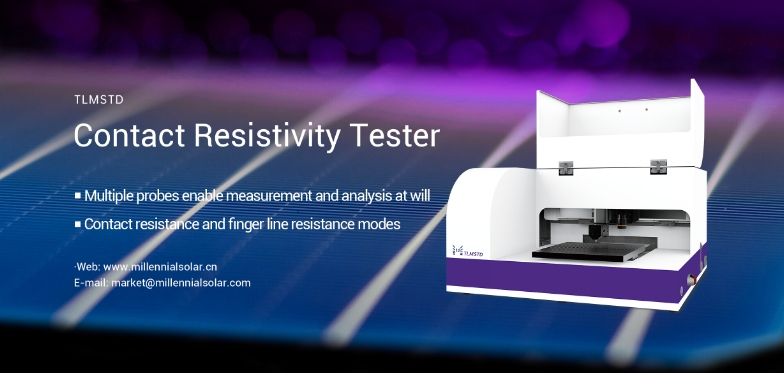
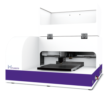
Contact Resistance Tester
Ultra depth of field 3D microscope
Auto Visual Tester
VMM PV Vision Measuring Machine
Solar Cell Horizontal Tensile Tester
Steady State Solar Simulator for Solar Cell
Solar Cell UV Aging Test Chamber
Solar Cell Comprehensive Tensile Tester
Visual Inspection Tester
Wet Leakage Current Tester
PV Module EL Tester
PV Module UV Preconditioning Chamber
Steady State Solar Simulator for PV Module
Current Continuous Monitor
Potential Induced Degradation Test
Bypass Diode Tester
LeTID Test System
Reverse Current Overload Tester
Impulse Voltage Tester
Hipot Insulation Tester
Ground Continuity Tester
Hipot Insulation Ground Tester
Damp Heat Test Chamber
Humidity Freeze Test
Thermal Cycle Test Chamber
Dynamic Mechanical Load Tester
Static Mechanical Load Tester
Hail Impact Tester
Robustness of Termination Tester
Module Breakage Tester
Cut Susceptibility Tester
Peel Shear Strength Tester
Universal Testing Machine (Single-arm)
Universal Testing Machine (Double-arm)
Glass Transmittance Tester
Acetic Acid Test Chamber
EVA Degree of Crosslinking Test System
Junction Box Comprehensive Tester
Drop ball tester
Semi-automatic scanning four-probe tester
Stylus Profilometer
Maximum Power Point Tracker
Perovskite Glass Transmittance Tester
Perovskite P1 Laser Scribing Multifunctional Testing Machine
Perovskite Online PL Tester
Perovskite Online Sheet Resistance Tester
Online Perovskite Film Thickness Tester
Perovskite Process Inspection Workstation
Portable EL Tester
Portable Thermal Imaging Tester
Solar Module Multi-Channel Testing System
PV Inverter Power Quality Tester
Drone EL Tester
IV Tester
IVEL Cell Sorting Machine
Application of LECO in TOPCon Cell Manufacturing Process
Date : 31 January 2024Views : 9655
LECO, also known as Laser Enhanced Contact Optimization, is an advanced laser sintering process that locally destroys the passivation layer in a very precise manner and promotes electron transfer between metal and silicon. TOPCon solar cells using LECO technology can increase conversion efficiency by 0.2%-0.5%. TLM Contact Resistivity Tester can measure problems in contact resistivity, reaction diffusion, electrode production, sintering and other processes, and protects the research and development of advanced cell technology.
The impact of sintering process on solar cell performance
TOPCon solar cells are in the transition stage to industrial mass production. On the back is the eponymous tunnel oxide passivation contact layer (TOPCon), phosphorus doped (n-type Cz-Si), and on the front is a conventional diffused boron emitter (p+). Currently, the main loss mechanism of TOPCon solar cells is the reorganization caused by the metal electrode of JOe-met on the emitter side, while the degree of reorganization caused by the metal electrode of JOT-met on the TOPCon side is lower.
The contact formation process is carried out industrially using conveyor belt furnaces (FFOs), typically at peak temperatures above 700°C, where the dielectric capping layer covered by screen-printed electrodes is etched.
Then, the oxygen ions on both sides react with the crystal or polysilicon, promoting the creation of ohmic contact. On the front side, the locally removed passivation layer greatly increases recombination. On the backside, etch pits consume the polysilicon and may reach thin oxide layers, passivating the contacts. The contact formation process on both sides is driven by the increased combustion temperature. On the one hand, this results in a high fill factor FF; on the negative side, this leads to an increase in metal-induced recombination, mainly reducing Voc, ultimately limiting the improvement in conversion efficiency.
Use LECO as a post-sinter treatment to lower the contact firing temperature to achieve higher Voc and FF values on TOPCon solar cells.
Introduction to LECO process
The LECO process applies high-intensity laser pulses locally on the front side of the solar cell and maintains a constant reverse voltage. The resulting local currents significantly reduce the contact resistivity between the semiconductor and metal electrodes.
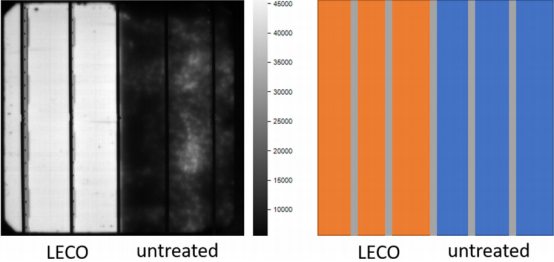
right side(without LECO), left side(image of the EL and contact resistance after treatment)
The specific process flow is as follows:
A. Preparation: First, the silicon solar cells complete the deposition of the passivation layer through conventional process steps to form a high-quality passivation layer to reduce surface recombination.
B. Silver paste printing: Use screen printing or other printing techniques to apply silver paste on the front surface of the silicon wafer to form a predetermined electrode pattern. Silver paste contains silver particles as well as organic solvents and binders.
C. Pre-drying: Before laser processing, the silicon wafer coated with silver paste is pre-dried to remove most of the organic solvent and avoid gas bubbles generated during laser heating from affecting the contact quality.
D. Sintering: By precisely controlling the energy and irradiation time of the laser, the laser irradiates the silver paste and locally heats the silver paste for sintering. The thermal effect of the laser induces the melting and joining of the silver particles in the silver paste.
During this process, the microscopic changes between the silver paste and the cells are as follows:
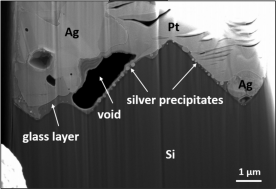
SEM image of contact cross-section without LECO treatment
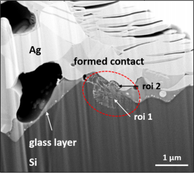
SEM image of contact cross-section after LECO treatment
a. Local destruction of passivation layer: The hot spot caused by laser heating will locally destroy the passivation layer on the silicon wafer. This is a precisely controlled physical process. The purpose of destroying the passivation layer is to enable the silver to form direct contact with the silicon wafer and establish an effective electron transmission path.
b. Formation of silver-silicon alloy: Under the action of high temperature, silver particles begin to react with silicon to locally form a silver-silicon alloy. This process involves the diffusion of silver atoms into the silicon wafer surface and the formation of good ohmic contact in the contact area.
E. Cooling and solidification: After laser treatment, the sintered area begins to cool. The metallic connections between the silver particles solidify, forming a strong electrode.
F. Cleaning and Inspection: Finally, the processed wafers are cleaned to remove any residual organic matter and inspected to ensure contact quality and cell functionality.
Throughout the LECO process, changes at the microscopic level are critical to solar cell performance. The interaction between the silver paste and the silicon wafer surface needs to be precisely controlled to ensure that contact resistance is minimized while avoiding unnecessary structural damage to the silicon wafer.
Contact Resistivity Tester
E-mail: market@millennialsolar.com
Contact Resistivity Tester can quickly, flexibly and accurately measure the contact resistance and line resistance. Reflects problems existing in processes such as diffusion, electrode production, and sintering.
Contact resistivity test range: 0.1~120mΩ*cm^2;
Line resistance test range: 0.2~40Ω/cm
Contact resistivity measurement accuracy: 5% or 0.5mΩ*cm^2
Line resistance measurement accuracy: 5% or 0.1Ω/cm
Static test repeatability ≤1%, dynamic test repeatability ≤3%
LECO process can do more than simply improve the average solar cell performance, it also allows for overall fine-tuning of the entire process sequence and the achievement of more uniform contact resistivity. LECO has been proven to be used in TOPCon solar cells, which can increase conversion efficiency by 0.2%-0.5%. Millennial Solar provides high-precision testing equipment for measuring solar cell contact resistance and line resistance. We focus on technological innovation, assists the iterative development of solar cell technology, and improves the power generation efficiency and economy of photovoltaic products.


