
Quantum Efficiency Tester
PL/EL Integrated System
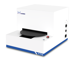
PV-Reflectumeter
3D Confocal Microscope
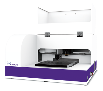
In-Line Four Point Probe Tester
Four Point Probe Tester
In-Line Thin Film Thickness Tester
Raman Spectrometer
FTIR Spectrometer
Spectrophotometer
Automatic Spectroscopic Ellipsometer
Contact Resistance Tester
Ultra depth of field 3D microscope
Auto Visual Tester
VMM PV Vision Measuring Machine
Solar Cell Horizontal Tensile Tester
Steady State Solar Simulator for Solar Cell
Solar Cell UV Aging Test Chamber
Solar Cell Comprehensive Tensile Tester
Visual Inspection Tester
Wet Leakage Current Tester
PV Module EL Tester
PV Module UV Preconditioning Chamber
Steady State Solar Simulator for PV Module
Current Continuous Monitor
Potential Induced Degradation Test
Bypass Diode Tester
LeTID Test System
Reverse Current Overload Tester
Impulse Voltage Tester
Hipot Insulation Tester
Ground Continuity Tester
Hipot Insulation Ground Tester
Damp Heat Test Chamber
Humidity Freeze Test
Thermal Cycle Test Chamber
Dynamic Mechanical Load Tester
Static Mechanical Load Tester
Hail Impact Tester
Robustness of Termination Tester
Module Breakage Tester
Cut Susceptibility Tester
Peel Shear Strength Tester
Universal Testing Machine (Single-arm)
Universal Testing Machine (Double-arm)
Glass Transmittance Tester
Acetic Acid Test Chamber
EVA Degree of Crosslinking Test System
Junction Box Comprehensive Tester
Drop ball tester
Semi-automatic scanning four-probe tester
Stylus Profilometer
Maximum Power Point Tracker
Perovskite Glass Transmittance Tester
Perovskite P1 Laser Scribing Multifunctional Testing Machine
Perovskite Online PL Tester
Perovskite Online Sheet Resistance Tester
Online Perovskite Film Thickness Tester
Perovskite Process Inspection Workstation
Portable EL Tester
Portable Thermal Imaging Tester
Solar Module Multi-Channel Testing System
PV Inverter Power Quality Tester
Drone EL Tester
IV Tester
IVEL Cell Sorting Machine
Effect of Phosphorus Doping Time on Reflectivity, Contact Resistance and Sheet Resistance of Crystal
Date : 1 April 2024Views : 1700
Crystalline silicon solar cells are one of the major solar cell technologies currently on the market, in which the metallization of silicon wafers plays a vital role in effectively collecting solar energy. The contact formation and characteristics between the silicon wafer and the metal gate line are affected by the doping level of the PN junction. The impact of the doping concentration on the cell performance can be judged by measuring the sheet resistance. The contact resistance between the cell and the metal gate line can be judged by measuring the quality of contact resistance. These tests play a leading role in improving solar cell performance. Millennial Solar can provide PV-Reflectometer, Contact Resistance Tester and (In-Line) Four Point Probe Tester to meet the testing needs of users, enabling precise control of various parameters of solar cells during the production process and providing customers with a variety of options.
Analysis of the influence of doping rate on solar cell surface reflectance
To create efficient crystalline silicon solar cells, optical surface reflections can be reduced by forming evenly distributed pyramid structures on the surface of the silicon wafer. The lower optical reflectivity mainly depends on the shape, size and uniformity of the pyramids on the silicon wafer surface. These pyramid structures are controlled by etch rate, potassium hydroxide (KOH), and isopropyl alcohol (IPA), where the etch rate affects the formation of pyramids, KOH affects the number of pyramids, and isopropyl alcohol affects the size of the pyramids.
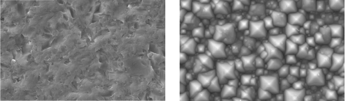
SEM images of original silicon wafer (left) and silicon wafer after cleaning and texturing process (right)
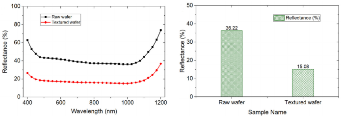
Comparison of reflectance versus wavelength curves (left) and reflectivity percentage (right) of original silicon wafers and silicon wafers after cleaning and texturing.
Analysis of the Effect of Doping Time on Film Sheet Resistance
In the photovoltaic industry, the sheet resistance of the film is critical to cell performance as it indicates the quality and uniformity of the PN junction doped area. A higher sheet resistance represents light doping, which will cause the silicon wafer contact resistance to be too high, while a low sheet resistance represents heavy doping, which will cause the silicon wafer contact resistance to be too low.
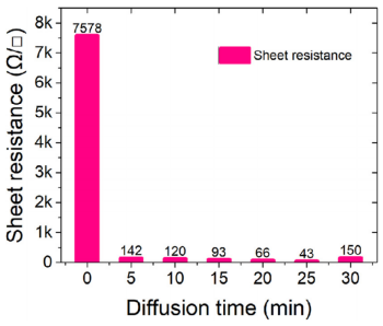
Changes in sheet resistance values of 5 groups of silicon wafers as diffusion time increases
It can be observed from the figure above that the sheet resistance value of silicon wafers doped with phosphorus atoms is significantly reduced. The sheet resistance before diffusion is 7578Ω/□. As the diffusion time increases, the sheet resistance values of the five groups of silicon wafers decrease rapidly until the value of sheet resistance is minimum at 25 minutes. This is because as the diffusion time increases, the doping concentration of phosphorus atoms also increases, and the sheet resistance value is inversely proportional to the doping concentration. At 30 minutes, the square resistance value began to increase again, which was due to over-doping.
Analysis of the influence of doping time on solar cell contact resistance
Contact resistance is affected by three main factors, namely semiconductor material, doping concentration and conductor material type. Doping concentration is an important factor in controlling contact resistance. Higher doping concentration will significantly reduce contact resistance. However, when the concentration of phosphorus atoms exceeds the solid solubility limit of the silicon wafer, a "dead layer" will be formed on the semiconductor surface. By rendering the silicon wafer electrically inactive, it also acts as a recombination center, hindering the conversion efficiency of the solar cell.
By doping six cell samples with phosphorus atoms respectively, the time changes were 5min, 10min, 15min, 20min, 25min and 30min respectively, and the contact resistance of the six areas on the front and back surfaces of the cell was measured.
Table 1. Front surface contact resistance values of 6 samples
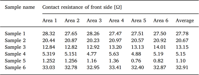
Table 2. Back contact resistance values of 6 samples
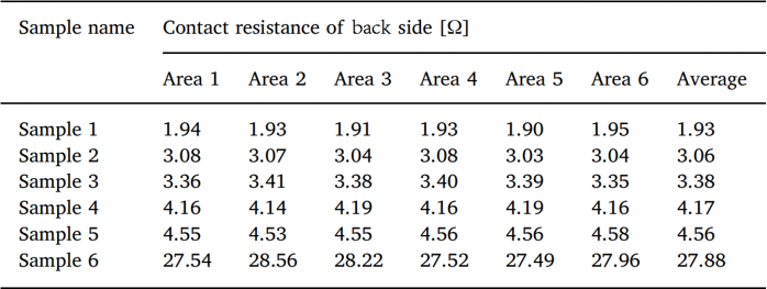
From the above two sets of data, it can be concluded that the contact resistance of the front surface decreases as the phosphorus doping time increases, but when it reaches 30 minutes, a "dead layer" is formed on the surface of the silicon wafer and the contact resistance value increases. The contact resistance value of the back surface is different from that of the front surface. It also increases slowly with the increase of doping time until it starts to rise sharply after 25 minutes. The reason may be that the solid solubility of phosphorus atoms in silicon wafers exceeds the limit.
Therefore, the diffusion time of 25 minutes can be regarded as the optimal time, which is beneficial to the production of high-efficiency crystalline silicon solar cells.
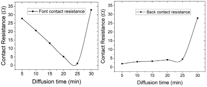
Contact resistance versus diffusion time curves for front (left) and back (right) solar cells
PV-Reflectometer
E-mail: market@millennialsolar.com
PV-Reflectometer is an important helper for process inspection of solar cell manufacturers. You can test the reflectivity intensity of the textured sample to light of different wavelengths, excite the cell through diffuse reflection, and detect it with a spectrometer at an 8-degree angle. RTIS has a positioning machine platform and guide rails, which can conveniently and quickly position cell samples and improve the work efficiency of users.
Contact Resistance Tester
E-mail: market@millennialsolar.com
Contact Resistance Tester can quickly, flexibly and accurately measure the contact resistance and line resistance of solar cells. Reflects problems existing in processes such as diffusion, electrode production, and sintering.
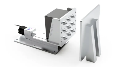
Four Point Probe Tester
E-mail: market@millennialsolar.com
Four Point Probe Tester can quickly and automatically scan samples up to 230mm to obtain sample resistance/resistivity distribution information. It can be widely used in photovoltaics, semiconductors, alloys, ceramics and many other fields.
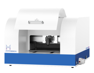
In-Line Four Point Probe Tester
E-mail: market@millennialsolar.com
FPP230 Auto is an In-Line Four Point Probe Tester specially designed for process monitoring. The device can quickly and automatically scan the sample to obtain the sheet resistance distribution information at different positions of the sample. The measurement size can be customized according to the size of the customer's sample.
By changing the phosphorus doping time in the PN junction region, the surface reflectivity, contact resistance and sheet resistance of the solar cell can be changed, which contributes to the preparation of high-efficiency crystalline silicon solar cells. Millennial Solar provides users with PV-Reflectometer, Contact Resistance Tester and (In-Line) Four Point Probe Tester to help users accurately control various parameters of solar cells during this process and jointly contribute to the development of the industry.


