
Quantum Efficiency Tester
PL/EL Integrated System
PV-Reflectumeter
3D Confocal Microscope
In-Line Four Point Probe Tester
Four Point Probe Tester
In-Line Thin Film Thickness Tester
Raman Spectrometer
FTIR Spectrometer
Spectrophotometer
Automatic Spectroscopic Ellipsometer
Contact Resistance Tester
Ultra depth of field 3D microscope
Auto Visual Tester
VMM PV Vision Measuring Machine
Solar Cell Horizontal Tensile Tester
Steady State Solar Simulator for Solar Cell
Solar Cell UV Aging Test Chamber
Solar Cell Comprehensive Tensile Tester
Visual Inspection Tester
Wet Leakage Current Tester
PV Module EL Tester
PV Module UV Preconditioning Chamber
Steady State Solar Simulator for PV Module
Current Continuous Monitor
Potential Induced Degradation Test
Bypass Diode Tester
LeTID Test System
Reverse Current Overload Tester
Impulse Voltage Tester
Hipot Insulation Tester
Ground Continuity Tester
Hipot Insulation Ground Tester
Damp Heat Test Chamber
Humidity Freeze Test
Thermal Cycle Test Chamber
Dynamic Mechanical Load Tester
Static Mechanical Load Tester
Hail Impact Tester
Robustness of Termination Tester
Module Breakage Tester
Cut Susceptibility Tester
Peel Shear Strength Tester
Universal Testing Machine (Single-arm)
Universal Testing Machine (Double-arm)
Glass Transmittance Tester
Acetic Acid Test Chamber
EVA Degree of Crosslinking Test System
Junction Box Comprehensive Tester
Drop ball tester
Semi-automatic scanning four-probe tester
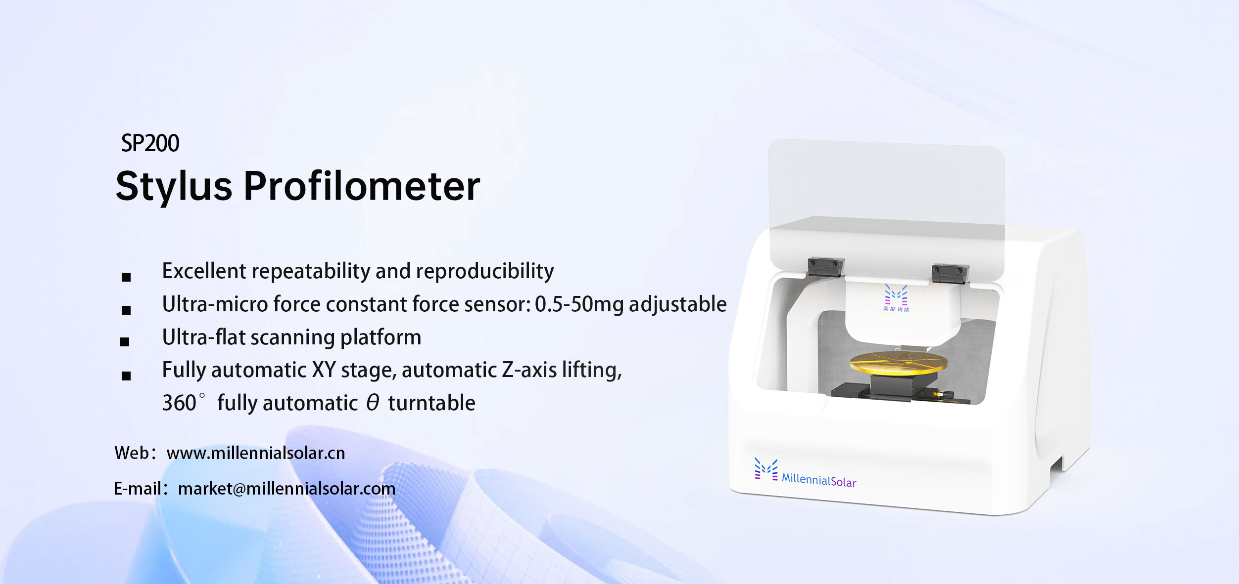
Stylus Profilometer
Maximum Power Point Tracker
Perovskite Glass Transmittance Tester
Perovskite P1 Laser Scribing Multifunctional Testing Machine
Perovskite Online PL Tester
Perovskite Online Sheet Resistance Tester
Online Perovskite Film Thickness Tester
Perovskite Process Inspection Workstation
Portable EL Tester
Portable Thermal Imaging Tester
Solar Module Multi-Channel Testing System
PV Inverter Power Quality Tester
Drone EL Tester
IV Tester
IVEL Cell Sorting Machine
Perovskite Solar Cells: Optimizing Film Quality and Accurate Thickness Measurement
Date : 5 June 2024Views : 1990
The performance of perovskite solar cells is affected by the quality and thickness of the film. High-quality films improve the efficiency of electron and hole transfer, reduce energy loss and extend carrier lifetime. Optimizing the preparation process, such as using low-toxic solvents and closed steam annealing, can improve the crystallinity and uniformity of the film and improve the photoelectric conversion efficiency (PCE). This article discusses the application of NEP solvents in film preparation and the effect of closed steam annealing on grain growth. In particular, the key role of the Millennial Stylus Profilometer in measuring film thickness and surface morphology is introduced. These technologies are expected to promote the development of high-efficiency perovskite solar cells.
Thin film quality and thickness are key factors affecting the actual device fabrication performance of perovskite solar cells
The quality of perovskite films directly affects the photoelectric conversion efficiency (PCE) of solar cells. High-quality perovskite films have large crystal grains, which are beneficial to the rapid transmission of electrons and holes, reduce energy loss, and increase the lifetime of carriers. In addition, by optimizing the preparation process, such as using low-toxic solvents and closed steam annealing methods, the crystallinity and uniformity of perovskite films can be significantly improved, thereby improving the PCE of solar cells.
For example, in the preparation of high-quality organic-inorganic perovskite films and research experiments on solar cells, focusing on the key issue of preparing high-quality perovskite films, green and low-toxicity solvents are selected, and the solvents are used to form the perovskite film. A series of studies have been carried out on its role in .
By adding NEP solvent and using closed vapor annealing, columnar crystals can be obtained to facilitate the rapid transport of electrons and holes while hindering their recombination, increasing the PCE of the solar cell from 12.3% to 16.8%.
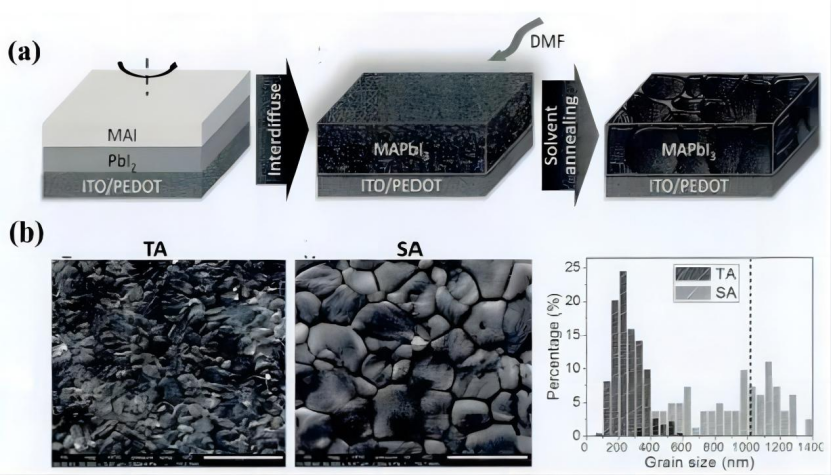
Schematic diagram of solvent annealing; (b) SEM images of films prepared by solvent annealing (SA) and traditional annealing (TA)
Combining the Lewis acid-base and dissolution-recrystallization theory, a low-toxic NEP solvent is introduced into the Pbl₂/PbBr₂/DMF solution in the first step of the two-step solution spin coating method, first forming a Lewis acid-base compound Pbl₂·Sol (Sol=DMF, NEP), and then the compound reacts with CH(NH₂)₂I and CH₃NH₃Br to form a perovskite intermediate phase. Pbl₂·NEP not only provides a channel for the diffusion of FAI/MABr, but also the strong interaction between the additive NEP and Pbl₂ delays the reaction of Pbl₂ with FAI/MABr. The slow reaction helps the growth of grains, thereby improving the surface morphology of the perovskite film. In addition, a closed steam annealing method is used to dissolve and recrystallize the perovskite film with the help of the evenly distributed residual solvent in the perovskite intermediate phase, further promoting the secondary growth of grains. Based on the dual effects of the solvent, the average grain size of the perovskite film increased from 205nm to 718nm, and the average carrier lifetime increased from 155ns to 561ns. Ultimately, a high-quality perovskite film with good crystallinity, few defects, long carrier lifetime, and columnar grains was prepared, thereby increasing the photoelectric conversion efficiency of solar cells from 10.8% to 17.0%. Millennial Stylus Profilometer automatically measures multiple points at different positions to confirm the exact thickness of the film on the entire silicon surface, and provides accurate measurement without contact damage.
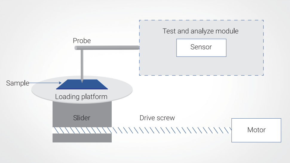
Stylus Profilometer contact surface topography measurement principle
Stylus Profilometer mainly achieves precision measurement through the tiny up and down movement of the stylus when it moves on the surface of the detected object. When the stylus slides on the surface, the tiny peaks and valleys on the surface cause the stylus to move up and down. This movement reflects the contour of the surface to a certain extent. The sensor converts the displacement of the equilibrium position of the stylus into an electrical signal and measures it through a bridge. The output signal is proportional to the displacement of the equilibrium position of the stylus. After amplification and rectification, the displacement signal is demodulated and finally read in the controller. The signal is further processed by noise filters and waviness filters to reduce the influence of errors on the measurement results.
From the perspective of elastic contact, Hertz-Mindlin contact is an important theoretical basis that considers the overall behavior of rough interfaces and the interaction between asperities on the interface. This theoretical model includes not only elastic deformation but also frictional sliding, which is critical for understanding and predicting the force-deformation behavior of contact surfaces. In addition, the Hertz theory is also used to describe the relationship between normal force and feeding level under non-adhesive contact.
Second, for plastic contact, it is traditionally believed that the actual contact area between two nominally flat metal surfaces is determined by the plastic deformation of their highest convexity. This assumption leads to the result that the actual contact area is directly proportional to the load and is independent of the surface significant area.
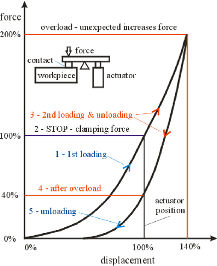
Typical characteristics of the contact between the rough surface of the workpiece and the fixture
In addition, experimental studies have also shown that in flat surface contact, the ratio of elastic and plastic deformation depends on the strength parameters of the specimen and the roughness parameters of the contact surface. Millennial Stylus Profilometer's new probe-type surface profile measurement technology can accurately measure film height, step height, 2D morphology, surface roughness and other parameters.
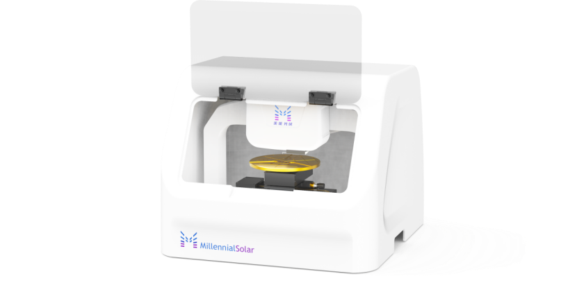
Millennial Stylus Profilometer
E-mail: market@millennialsolar.com
Millennial Stylus Profilometer uses contact-type surface topography measurement, which can confirm the accurate thickness of the film through multi-point automatic measurement at different positions.
● Equipped with a 500W pixel high-resolution color camera
● Sub-angstrom resolution, step height repeatability 1nm
● 360° rotating θ platform combined with Z-axis lifting platform
● Ultra-micro force constant force sensor ensures accurate measurement without contact damage
By optimizing the preparation process of the perovskite film, the crystallinity and uniformity of the film are significantly improved, and the photoelectric conversion efficiency of the solar cell is improved. Millennial Stylus Profilometer plays a key role in the precise measurement of film thickness and surface morphology.


