
Quantum Efficiency Tester
PL/EL Integrated System
PV-Reflectumeter
3D Confocal Microscope
In-Line Four Point Probe Tester
Four Point Probe Tester
In-Line Thin Film Thickness Tester
Raman Spectrometer
FTIR Spectrometer
Spectrophotometer
Automatic Spectroscopic Ellipsometer
Contact Resistance Tester
Ultra depth of field 3D microscope
Auto Visual Tester
VMM PV Vision Measuring Machine
Solar Cell Horizontal Tensile Tester
Steady State Solar Simulator for Solar Cell
Solar Cell UV Aging Test Chamber
Solar Cell Comprehensive Tensile Tester
Visual Inspection Tester
Wet Leakage Current Tester
PV Module EL Tester
PV Module UV Preconditioning Chamber
Steady State Solar Simulator for PV Module
Current Continuous Monitor
Potential Induced Degradation Test
Bypass Diode Tester
LeTID Test System
Reverse Current Overload Tester
Impulse Voltage Tester
Hipot Insulation Tester
Ground Continuity Tester
Hipot Insulation Ground Tester
Damp Heat Test Chamber
Humidity Freeze Test
Thermal Cycle Test Chamber
Dynamic Mechanical Load Tester
Static Mechanical Load Tester
Hail Impact Tester
Robustness of Termination Tester
Module Breakage Tester
Cut Susceptibility Tester
Peel Shear Strength Tester
Universal Testing Machine (Single-arm)
Universal Testing Machine (Double-arm)
Glass Transmittance Tester
Acetic Acid Test Chamber
EVA Degree of Crosslinking Test System
Junction Box Comprehensive Tester
Drop ball tester
Semi-automatic scanning four-probe tester
Stylus Profilometer
Maximum Power Point Tracker
Perovskite Glass Transmittance Tester
Perovskite P1 Laser Scribing Multifunctional Testing Machine
Perovskite Online PL Tester
Perovskite Online Sheet Resistance Tester
Online Perovskite Film Thickness Tester
Perovskite Process Inspection Workstation
Portable EL Tester
Portable Thermal Imaging Tester
Solar Module Multi-Channel Testing System
PV Inverter Power Quality Tester
Drone EL Tester
IV Tester
IVEL Cell Sorting Machine
Edge Etching Process After Diffusion Junction of Solar Cells
Date : 1 August 2024Views : 1830
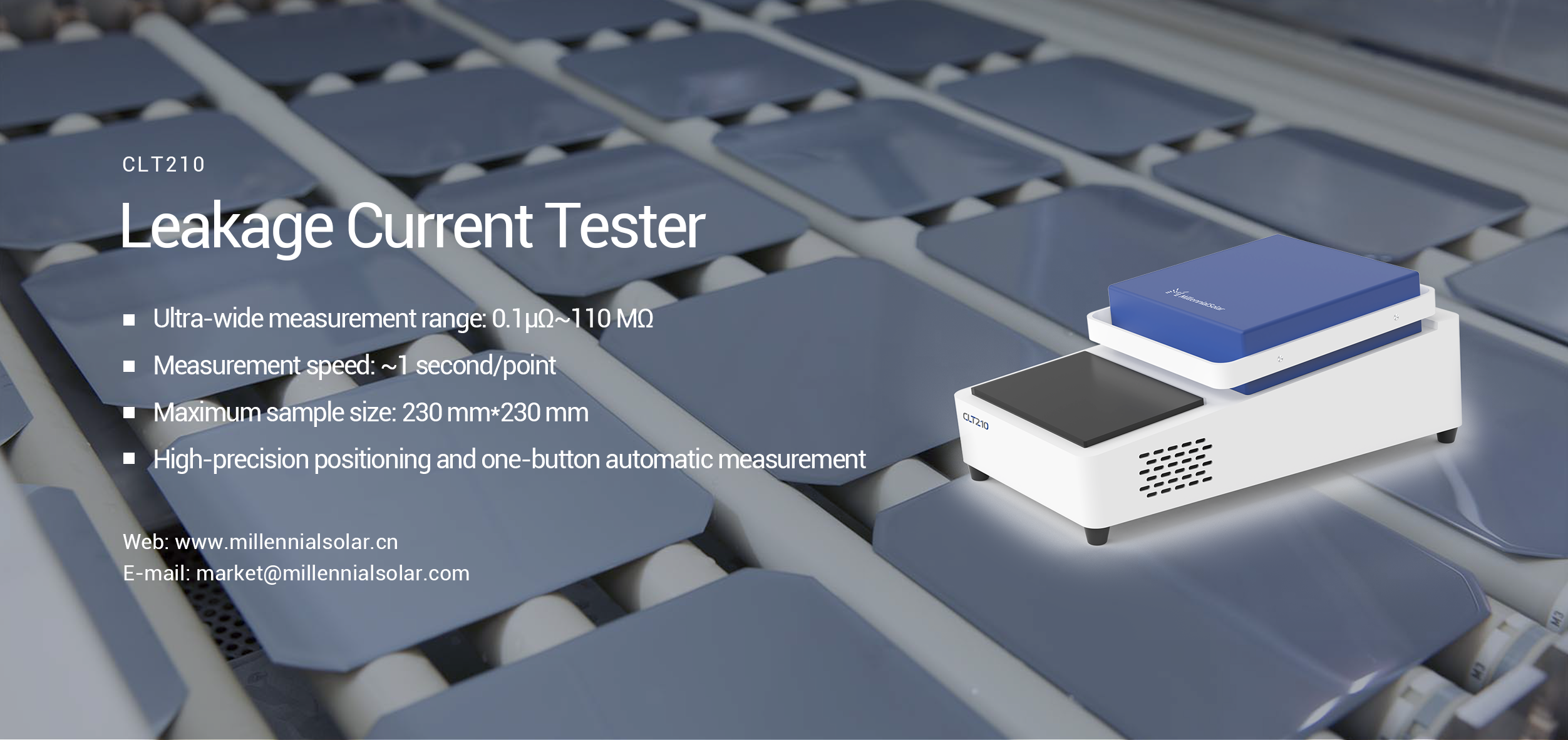
Tunneling oxide passivation contact (TOPCon) technology still attracts a lot of attention from photovoltaic industry manufacturers. However, in the production process, the battery will encounter problems with wrap-around plating and edge leakage current. These phenomena will lead to a decrease in the optical and electrical performance of the battery, such as open circuit voltage (Voc), short circuit current density (Jsc) and fill factor (FF). Millennial CLT210 is a leakage current tester designed for RCA process research. It can quickly and automatically measure samples below 230mm, obtain sample edge leakage current information, and help manufacturers improve problems such as wrap-around plating and edge leakage current in the production process.
Diffusion layer and impurity layer formed on the back and edge of silicon wafer after diffusion
After diffusion bonding, a diffusion layer and silicon dioxide layer will be formed on the surface of the silicon wafer (including the front, back and edges). At present, most manufacturers on the market use single-sided diffusion, that is, silicon wafers are placed in pairs with backs attached to backs, but the diffusion impurity gas will still pass through the gaps between the silicon wafers, so impurities will inevitably diffuse into the other side of the silicon wafer.

TOPCon process flow
When making a PN junction on a P-type silicon wafer, the diffused impurity is phosphorus. The P2O5 produced by the decomposition of POCl3 is deposited on the surface around the silicon wafer, forming a mixture of phosphorus atoms, silicon dioxide, and P2O5 - phosphosilicate glass (PSG). When making a PN junction on an N-type silicon wafer, borosilicate glass (BSG) is formed during the diffusion process. The removal process of the two impurity layers is similar.
When solar cells are actually used, the photogenerated carriers generated by light on the front of the cell will flow along the diffusion layer and impurity phosphosilicate glass layer on the edges to the back of the cell, thereby reducing the parallel resistance of the solar cell and causing an electrode short circuit.
Therefore, the diffusion layer and phosphosilicate glass layer PSG on the back and edges of the solar cell must be removed.
Three edge etching process methods
1. Plasma etching
Currently, plasma etching methods are basically only used in laboratories and are no longer used in actual production processes. This method usually removes the residual native oxide or diffused oxide by chemical means first, and then neatly "stacks" the silicon wafers, similar to stacking coins. The stacked silicon wafers are then placed in a plasma chamber. Currently, most use CF4+O2 or SF4+O2 as the reaction gas. The corrosive ion gas generated etches the exposed edges of the stacked silicon wafers, thereby effectively removing the diffused silicon at the edges.
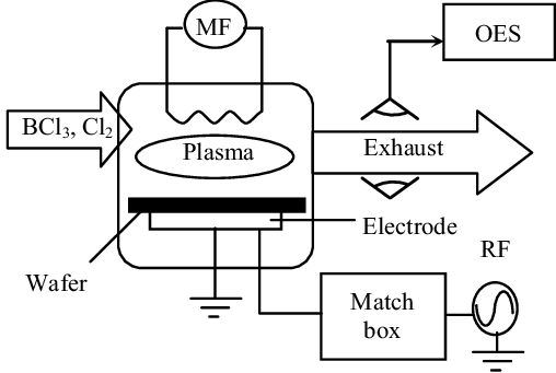
Schematic diagram of plasma etching
The advantages of this method are fast etching rate and isotropy, and the morphology of the silicon wafer will not be changed after etching. However, the etching time needs to be strictly controlled. A shorter etching time will lead to insufficient etching, and impurities at the edge will not be removed cleanly, resulting in a decrease in the parallel resistance of the PN junction or even a short circuit. A longer time will cause excessive damage to the edge of the silicon wafer, thereby damaging the PN junction and forming a high recombination area.
2. Laser edge etching isolation
Laser edge etching isolation, also known as laser scribing, uses laser to ablate the front edge of the solar cell to form a closed groove with a certain depth, thereby effectively cutting off the current path to the edge and achieving isolation and insulation between the front electrode and the PN junction on the back of the solar cell. Unlike other processes, laser doping edge isolation is performed after screen printing the paste and sintering.
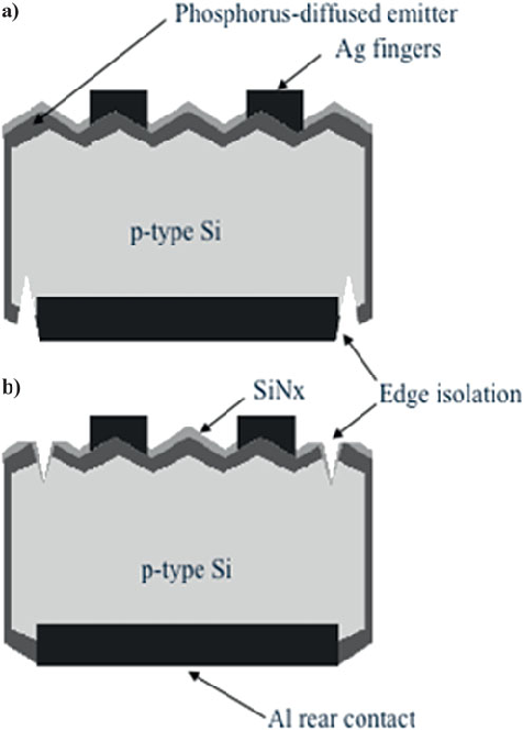
Laser edge isolation schematic
The laser edge etching isolation process itself cannot improve the conversion efficiency of solar cells, but it can significantly reduce efficiency loss compared with other processes.
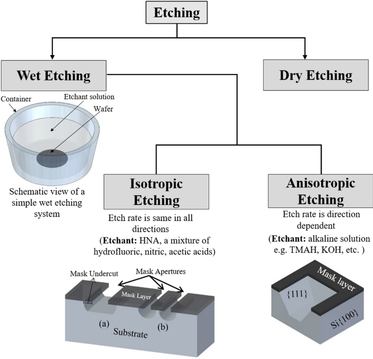
The above two processes are dry etching edge methods, while wet etching removes unnecessary impurities through solution etching.
3. Wet etching
Wet etching of the diffusion layer is to oxidize the back and edge of the silicon wafer with nitric acid to form silicon dioxide. Hydrofluoric acid reacts with silicon dioxide to form a complex hexafluorosilicic acid, while removing the diffusion layer and the phosphorus silicon glass layer PSG. The main reaction formula is as follows:
HNO3+Si→SiO2+NOX↑+H2O
SiO2+4HF→SiF4+2H2O
SiO4+2HF→H2[SiF6]
2NO2+H2O→HNO3+HNO2
Si+4HNO2→SiO2+4NO+2H2O
HNO3+2NO+H2O→3HNO2
During the etching process, it is necessary to ensure that the front side of the solar cell, i.e. the PN junction, is not corroded. Under this requirement, the current silicon wafer roller-carrying liquid etching method is superior to the floating etching method.
Roller-carrying liquid etching process for microcrystalline silicon μc-Si:H film
The roller is used to bring the solution to the back and periphery of the silicon wafer for etching. The silicon wafer is dragged forward by the roller, and the liquid level is lower than the upper surface of the roller. The capillary action on the roller is used to adsorb the silicon wafer, so that the silicon wafer will not deviate from the position and direction when moving in the flowing solution.
The production process is divided into 9 steps: loading silicon wafers → water spraying → edge etching → rinsing → alkali (KOH) cleaning → rinsing → acid (HF) cleaning → rinsing → air knife drying → unloading silicon wafers
Etching process monitoring and detection
After the edge diffusion layer and surface glass layer of the silicon wafer are etched, the appearance surface inspection and conductive type inspection are required.
The appearance surface quality inspection adopts visual inspection and microscope observation. The conductive type can be detected by the rectification method. The metal probe contacts the semiconductor to play a rectifying role and form an asymmetric conductance. For n-type semiconductors, the metal probe points to the semiconductor as the conduction direction; for p-type semiconductors, the semiconductor points to the metal as the conduction direction. By detecting the resistance value around the edges of the silicon wafer, it is determined whether the conduction direction is correct.
Millennial Leakage Current Tester

E-mail: market@millennialsolar.com
Millennial Leakage Current Tester CLT210 can quickly and automatically measure samples below 230mm to obtain leakage current information at the edge of the sample. The probe head is made of gold-plated material to ensure high mechanical precision and long service life. Current test range: 0.1μΩ~110 MΩ can cover most application scenarios and meet the industry's monitoring needs for leakage current in the RCA section. It is the only instrument in the industry that can achieve quantitative and positioning functions for testing leakage current.
·Ultra-wide measurement range: 0.1μΩ~110 MΩ
·Measurement speed: ~1 second/point
·Maximum sample size: 230 mm*230 mm
·High-precision positioning one-button automatic measurement
In short, the current silicon wafer etching technology has been continuously improving. Various process methods have advantages and disadvantages, and are still being continuously improved. Correspondingly, relevant equipment is required to be tested after the process is completed to determine whether the diffusion layer and phosphorus silicon glass layer formed on the back and edge of the silicon wafer after diffusion are completely removed. Millennial CLT210 is a leakage current tester designed for RCA process research to help users strictly control process quality inspection.


