
Quantum Efficiency Tester
PL/EL Integrated System
PV-Reflectumeter
3D Confocal Microscope
In-Line Four Point Probe Tester
Four Point Probe Tester
In-Line Thin Film Thickness Tester
Raman Spectrometer
FTIR Spectrometer
Spectrophotometer
Automatic Spectroscopic Ellipsometer
Contact Resistance Tester
Ultra depth of field 3D microscope
Auto Visual Tester
VMM PV Vision Measuring Machine
Solar Cell Horizontal Tensile Tester
Steady State Solar Simulator for Solar Cell
Solar Cell UV Aging Test Chamber
Solar Cell Comprehensive Tensile Tester
Visual Inspection Tester
Wet Leakage Current Tester
PV Module EL Tester
PV Module UV Preconditioning Chamber
Steady State Solar Simulator for PV Module
Current Continuous Monitor
Potential Induced Degradation Test
Bypass Diode Tester
LeTID Test System
Reverse Current Overload Tester
Impulse Voltage Tester
Hipot Insulation Tester
Ground Continuity Tester
Hipot Insulation Ground Tester
Damp Heat Test Chamber
Humidity Freeze Test
Thermal Cycle Test Chamber
Dynamic Mechanical Load Tester
Static Mechanical Load Tester
Hail Impact Tester
Robustness of Termination Tester
Module Breakage Tester
Cut Susceptibility Tester
Peel Shear Strength Tester
Universal Testing Machine (Single-arm)
Universal Testing Machine (Double-arm)
Glass Transmittance Tester
Acetic Acid Test Chamber
EVA Degree of Crosslinking Test System
Junction Box Comprehensive Tester
Drop ball tester
Semi-automatic scanning four-probe tester
Stylus Profilometer
Maximum Power Point Tracker
Perovskite Glass Transmittance Tester
Perovskite P1 Laser Scribing Multifunctional Testing Machine
Perovskite Online PL Tester
Perovskite Online Sheet Resistance Tester
Online Perovskite Film Thickness Tester
Perovskite Process Inspection Workstation
Portable EL Tester
Portable Thermal Imaging Tester
Solar Module Multi-Channel Testing System
PV Inverter Power Quality Tester
Drone EL Tester
IV Tester
IVEL Cell Sorting Machine
Study on the Efficiency of Double-sided Textured Perovskite/Crystalline Silicon Tandem Solar Cells
Date : 2 August 2024Views : 1620
Perovskite/crystalline silicon tandem solar cells have a rich material stack, each of which has unique functionality. Understanding the optoelectronic properties of these materials is of great significance for improving the efficiency of tandem energy conversion, and is also the key to the development of efficient light collection and light absorption layer technology and cost reduction. Millennial Quantum Efficiency Tester is compatible with all types of photovoltaic cell measurement needs, with a spectral range of up to 300-2500nm, fully locking in the advantages and disadvantages of the cell, helping users optimize structural design, material configuration and process parameters, and improving cell conversion efficiency.
Monolithic perovskite/crystalline silicon two-terminal (2T) tandem solar cells, where wide bandgap perovskite is used as the top cell absorber material and crystalline silicon is used as the bottom cell, have achieved a certified PCE of up to 31.3%, surpassing the PCE record of single-junction silicon solar cells. Currently, most high-efficiency monolithic perovskite/crystalline silicon tandems are based on silicon bottom cells (≈250-300µm thick) with a flat front-side polished or sub-micron textured surface to be compatible with solution-processed perovskite films.
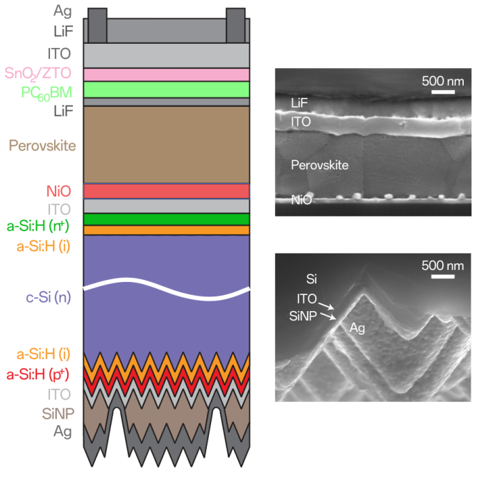
(Left) Schematic diagram of the structure of a perovskite/crystalline silicon tandem solar cell (Right) SEM images of the top and back cross-sections of a perovskite silicon tandem solar cell
Detailed optical analysis of perovskite/crystalline silicon tandem solar cells. Optical losses mainly come from reflection and parasitic absorption losses. The figure below shows the measured total absorbance, reflectivity and EQE of two subcells in a perovskite/crystalline silicon tandem solar cell.
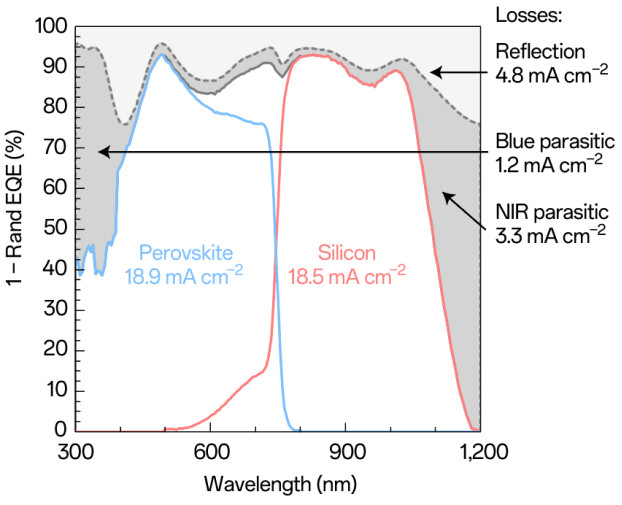
Measured total absorbance (reflectivity and EQE) of two subcells in a perovskite/silicon tandem solar cell
As shown in the figure, the perovskite top cell and the crystalline silicon bottom cell generate current densities of 18.9mA·cm-2 and 18.5mA·cm-2, respectively. The two main current losses come from front reflection (the area above the total absorbance curve) and parasitic absorption (the area between the total absorbance curve and the EQE curve), reaching 4.8mA·cm-2 and 3.3mA·cm-2, respectively. In order to further improve the current density of the stacked cell, the most direct way is to reduce the reflection on the front surface. Reflection can be reduced by anti-reflection layer, gradient refractive index and velvet light trapping structure.
Drawing on the technical route of crystalline silicon solar cells, the top cell of the perovskite/crystalline silicon stacked solar cell has moved from a planar structure to a pyramid textured surface structure, which can reduce reflection and increase light capture, thereby improving the energy conversion efficiency of the tandem solar cell.
A double-sided textured, production line compatible perovskite/silicon tandem solar cell
The hybrid hole transport layer (HTL) of NiOx/2PACz is obtained by applying an ultra-thin layer of 2PACz on a radio frequency (RF) sputtered NiOx layer. The sputtered dense NiOx layer can avoid the shunt path between the perovskite and the highly conductive TCO layer. At the same time, due to the strong chemical bonding between 2PACz and NiOx, 2PACz can be formed in a uniform conformal manner on the dense NiOx layer, and the surface defects of NiOx are also passivated.
Based on the designed NiOx/2PACz hybrid HTL, a monolithic 2T perovskite/crystalline silicon heterojunction stacked solar cell based on a production line compatible heterojunction bottom cell is fabricated. The TCO layer is located on a double-sided textured n-type crystalline silicon wafer with randomly distributed pyramidal morphology.
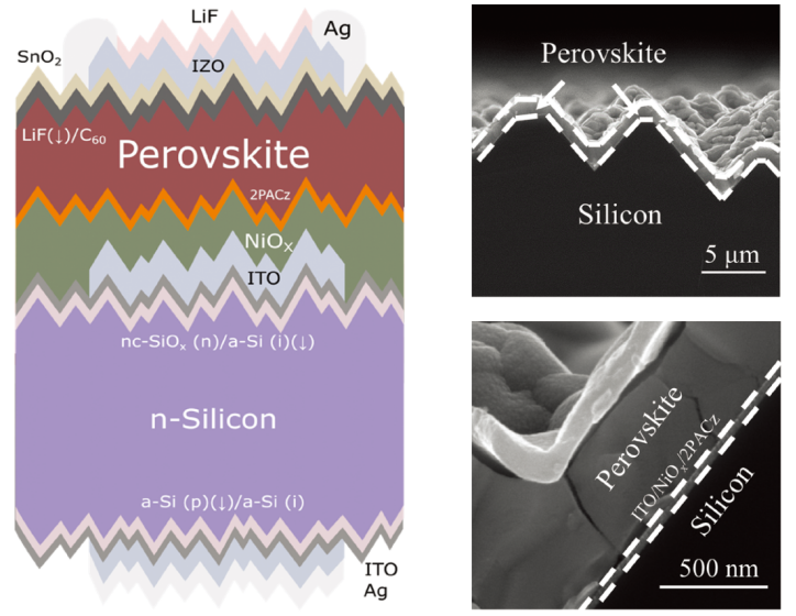
(Left) Schematic diagram of the structure of a double-sided velvet-structured perovskite/crystalline silicon tandem solar cell, (right) SEM image of the anti-reflection layer in the middle of the tandem cell
The figure below shows the measured total absorbance, reflectivity and EQE of the two sub-cells in the perovskite/crystalline silicon tandem solar cell made by this technology. The current density of the perovskite top cell and the crystalline silicon bottom cell increased to 19.75mA·cm-2 and 20.1mA·cm-2, respectively.
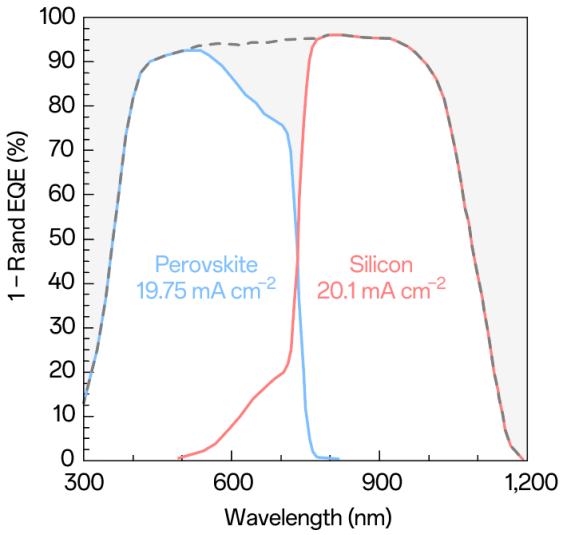
Measured total absorbance (reflectivity and EQE) of two subcells in a double-sided velvet-structured perovskite/silicon tandem solar cell
The discovery of this new technology also shows that by optimizing the surface morphology, the reflection and light escape of the front surface can be minimized, thereby enhancing the light capture ability and improving the PCE.
Optical light trapping principle of velvet structure
When light is incident on the surface of a material, reflection, refraction and transmission will occur. On a smooth surface, the reflected light and the incident light are on the same plane, and the reflection angle and the incident angle are the same. When the surface is rough, the interaction of light on the surface of the material will change. The change in the direction of adjacent surfaces causes the final reflection angle to be different from the incident angle.
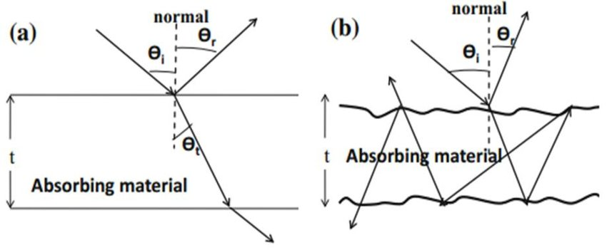
Schematic diagram of reflection, refraction, and transmission of light on a smooth surface (left) and a rough surface (right)
When parallel light falls on a smooth surface, the reflection angle is the same as the incident angle, and this reflection phenomenon is called specular reflection. At this time, the specular reflectivity is measured by placing the detector at the same angle as the incident angle to digitize the reflection phenomenon. When parallel light falls on a rough surface, reflection in random directions occurs, and this reflection is called diffuse reflection.
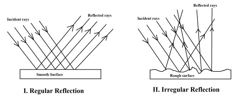
Schematic diagram of the reflection of parallel light on a smooth surface (left) and a rough surface (right)
Surface roughening not only changes the reflection angle, but also affects the refraction angle, so the propagation distance of light in the absorbing material increases. Surface roughening also helps to adjust the angle of incidence and achieve the condition of total internal reflection, which increases the optical path of the absorbing material.
For solar cells, the total reflectivity is the mirror reflection plus diffuse reflection. In order to measure this reflectivity, an integrating sphere is usually used to measure the reflectivity by collecting light from all directions to integrate and quantify the reflectivity.
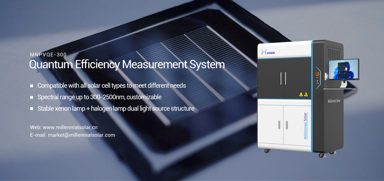
Quantum Efficiency Measurement System
E-mail: market@millennialsolar.com
MNPVQE-300 Quantum Efficiency Measurement System can measure the spectral response of all solar cells. The spectral range is from 300nm to 2500nm. It can measure parameters such as EQE, IQE, reflectivity, transmittance and short-circuit current density. It is equipped with a 150mm diameter integrating sphere to make your photovoltaic research progress more smoothly.
● Compatible with all types of solar cells to meet various testing needs
● The spectral range can reach 300-2500nm, and special customization is provided
● Xenon lamp + halogen lamp dual light source structure to ensure light source stability
This article details how to further improve the energy conversion efficiency of perovskite/crystalline silicon tandem solar cells by forming a velvet structure on the front surface to reduce light reflection. Millennial MNPVQE-300 Quantum Efficiency Measurement System is designed to provide data-based guidance for the development of high-performance functional layer optoelectronic materials, helping to maximize the spectral energy utilization of solar cells.


