
Quantum Efficiency Tester
PL/EL Integrated System
PV-Reflectumeter
3D Confocal Microscope
In-Line Four Point Probe Tester
Four Point Probe Tester
In-Line Thin Film Thickness Tester
Raman Spectrometer
FTIR Spectrometer
Spectrophotometer
Automatic Spectroscopic Ellipsometer
Contact Resistance Tester
Ultra depth of field 3D microscope
Auto Visual Tester
VMM PV Vision Measuring Machine
Solar Cell Horizontal Tensile Tester
Steady State Solar Simulator for Solar Cell
Solar Cell UV Aging Test Chamber
Solar Cell Comprehensive Tensile Tester
Visual Inspection Tester
Wet Leakage Current Tester
PV Module EL Tester
PV Module UV Preconditioning Chamber
Steady State Solar Simulator for PV Module
Current Continuous Monitor
Potential Induced Degradation Test
Bypass Diode Tester
LeTID Test System
Reverse Current Overload Tester
Impulse Voltage Tester
Hipot Insulation Tester
Ground Continuity Tester
Hipot Insulation Ground Tester
Damp Heat Test Chamber
Humidity Freeze Test
Thermal Cycle Test Chamber
Dynamic Mechanical Load Tester
Static Mechanical Load Tester
Hail Impact Tester
Robustness of Termination Tester
Module Breakage Tester
Cut Susceptibility Tester
Peel Shear Strength Tester
Universal Testing Machine (Single-arm)
Universal Testing Machine (Double-arm)
Glass Transmittance Tester
Acetic Acid Test Chamber
EVA Degree of Crosslinking Test System
Junction Box Comprehensive Tester
Drop ball tester
Semi-automatic scanning four-probe tester
Stylus Profilometer
Maximum Power Point Tracker
Perovskite Glass Transmittance Tester
Perovskite P1 Laser Scribing Multifunctional Testing Machine
Perovskite Online PL Tester
Perovskite Online Sheet Resistance Tester
Online Perovskite Film Thickness Tester
Perovskite Process Inspection Workstation
Portable EL Tester
Portable Thermal Imaging Tester
Solar Module Multi-Channel Testing System
PV Inverter Power Quality Tester
Drone EL Tester
IV Tester
IVEL Cell Sorting Machine
Advantages of UV Raman Spectroscopy in Crystallinity Analysis of Microcrystalline Silicon Thin Films
Date : 9 September 2024Views : 3600
The crystallinity (the proportion of crystal structure) of silicon thin films is crucial to the performance of photovoltaic cells. Since most silicon thin film characterization signals are masked by substrate signals, it is difficult to determine their crystallinity. Raman spectroscopy, ellipsometry, transmission electron microscopy (TEM) and other technologies are often used to measure the crystallinity of silicon thin films. Among them, Raman spectroscopy is the fastest. In just a few seconds, changes in wavelength or polarization can reveal relevant information about the sample. Millennial Raman Spectrometer is equipped with a 325 laser to optimize the design of the UV light path, improve spectral stability, and efficiently utilize the 325 laser and sample Raman signals to achieve in-situ testing of amorphous/microcrystalline materials above 5nm.
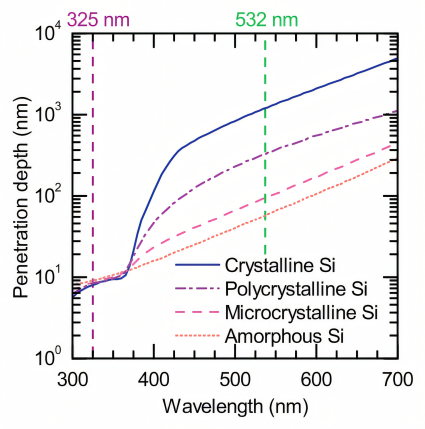
Light penetration depth in crystalline, polycrystalline, microcrystalline and amorphous silicon
Light penetration depth in crystal, polycrystalline, microcrystalline and amorphous silicon
Light penetration depth in crystal, polycrystalline, microcrystalline and amorphous silicon
We use 325 nm ultraviolet Raman excitation to analyze the crystallinity of silicon materials with different crystal structures. As shown in the figure, the penetration depth of 325 nm light in amorphous silicon film is only 8 nm, and the penetration depth in microcrystalline silicon film is 8.5 nm, which is almost the same. Commonly used Raman spectroscopy wavelengths include 514 and 532 nm, and the penetration depth of crystalline silicon and amorphous silicon differs by 10 times, which shows the difference in the penetration depth of light of different wavelengths in silicon materials.
The thickness range of amorphous silicon film that masks the underlying silicon wafer signal
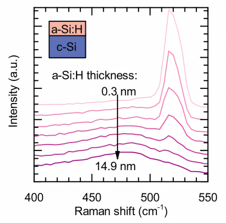
Raman spectra of amorphous silicon films of different thicknesses under 325nm excitation
As can be seen in the figure, for amorphous silicon films between 0.3nm and 12.6nm, the crystalline silicon peak from the underlying silicon wafer can be seen, but for films of 14.9nm (or thicker), it is not visible. The effect of the thickness of the amorphous silicon film on the appearance of the underlying silicon wafer signal in the Raman spectrum roughly determines the range of film thickness that can completely block the underlying silicon wafer signal.
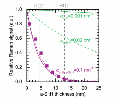
Effect of different thickness of amorphous silicon film on Raman signal
As shown in the figure, for 325nm excitation and amorphous silicon or microcrystalline silicon film, the Raman detection thickness (RDT) is 13nm, which means that films of 13nm or thicker can be analyzed by UV Raman, and films of 13nm thickness are more representative for Raman analysis.
Comparison of Raman spectra of microcrystalline silicon films on different substrates
Hydrogenated microcrystalline silicon films: 16.6 nm hydrogenated microcrystalline silicon films were prepared on c-Si and Al2O3 substrates, respectively.
Substrate treatment: Both were coated with 10 nm SiO2 (Raman transparent) deposited by PECVD to ensure the same growth of subsequent hydrogenated microcrystalline silicon layers.
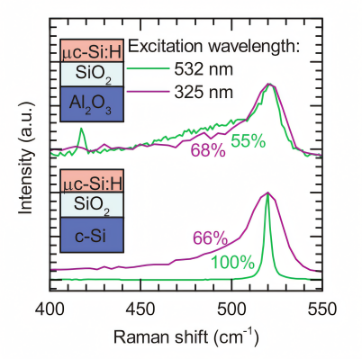
Raman spectra of 16.6nm thick microcrystalline silicon film on different substrates
Hydrogenated microcrystalline silicon film on SiO2/Al2O3 substrate: The crystallinity measured under 325nm excitation (68%) is slightly higher than that under 532nm excitation (55%), because the top of the film is easier to crystallize than the bottom, and the shorter wavelength (325nm) is more sensitive to the film surface.
Hydrogenated microcrystalline silicon film on SiO2/c-Si substrate: The 532nm Raman spectrum is strongly interfered by the silicon substrate signal, while the crystallinity measured by the 325nm Raman spectrum is almost the same as the result measured on SiO2/Al2O3 (66%).
This shows that the 325nm Raman spectrum is insensitive to the silicon substrate and is more suitable for analyzing the crystallinity of microcrystalline silicon films, while the 532nm Raman spectrum is interfered by the silicon substrate signal.
Relationship between crystallinity and thickness of microcrystalline silicon thin films

Crystallinity of microcrystalline silicon film - changes with film thickness
The figure above shows that the UV Raman crystallinity increases steadily with the increase of microcrystalline silicon film thickness, reaching a saturation of about 90% after 84nm, which reflects the dependence of film crystallinity on thickness.
For most films, the crystallinity determined by the ellipsometer is close to zero, while for films with a thickness of 24 and 84nm, the crystallinity jumps to more than 60%. This shows that the ellipsometer has certain difficulties in measuring crystallinity and it is difficult to accurately reflect the changes in the crystallinity of the film.
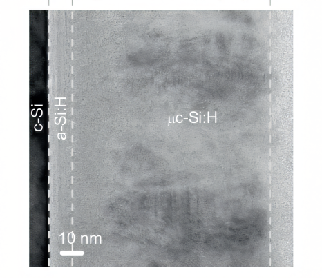
TEM image of the thickest (84nm) microcrystalline silicon film
TEM images are easier to convert into black and white contrast images for thicker films with conical crystals. UV Raman can be used to monitor the crystallinity of microcrystalline silicon films, and the data is qualitatively consistent with the obvious crystal areas in the TEM image.
In summary, UV Raman has advantages in measuring the crystallinity of microcrystalline silicon films and can more accurately reflect the relationship between the crystallinity and thickness of the film.
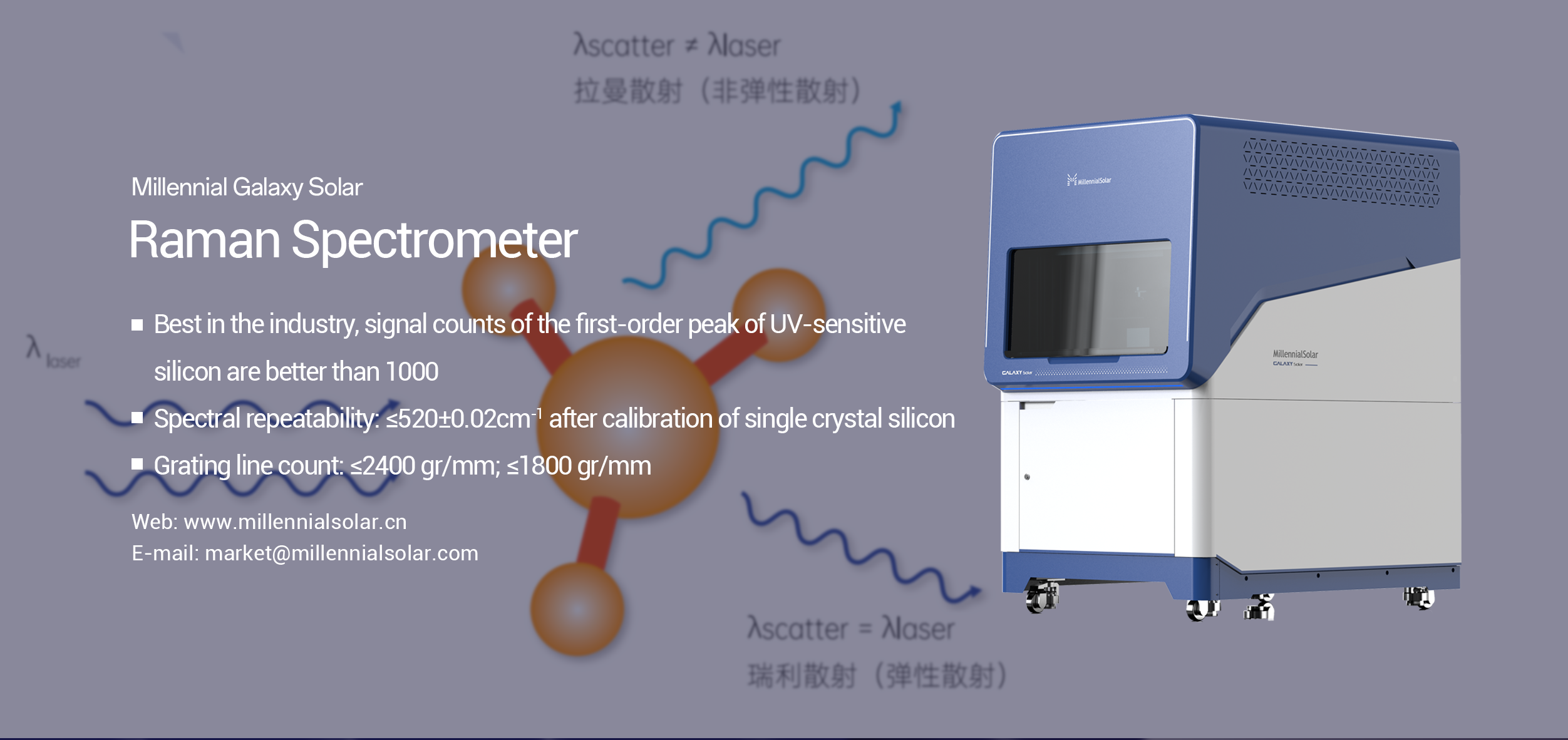
Raman Spectrometer
E-mail: market@millennialsolar.com
Raman Spectrometer has excellent UV sensitivity and excellent spectral repeatability. It uses 325 lasers, optimizes UV optical path design, improves spectral stability, and efficiently utilizes 325 lasers and sample Raman signals to achieve in-situ testing of amorphous/microcrystalline materials above 5nm. It is the best choice for characterizing "microcrystalline-heterojunction" cells.
· Industry best, UV sensitivity silicon first-order peak signal count is better than 1000 (1 second integration time)
·Spectral repeatability: after single crystal silicon calibration, ≤520±0.02cm-1
·Grating line count: ≤2400 gr/mm; ≤1800 gr/mm
Common Raman spectral wavelengths have problems when analyzing silicon thin films, while 325nm lasers have advantages when analyzing the crystallinity of thin silicon films. They have a suitable penetration depth in silicon materials and are insensitive to substrate signals. Raman Spectrometer uses a 325nm laser with a relatively shallow penetration depth, which can achieve in-situ testing of the crystallization rate and output the crystallization rate value with one click efficiently and accurately.


