
Quantum Efficiency Tester
PL/EL Integrated System
PV-Reflectumeter
3D Confocal Microscope
In-Line Four Point Probe Tester
Four Point Probe Tester
In-Line Thin Film Thickness Tester
Raman Spectrometer
FTIR Spectrometer
Spectrophotometer
Automatic Spectroscopic Ellipsometer
Contact Resistance Tester
Ultra depth of field 3D microscope
Auto Visual Tester
VMM PV Vision Measuring Machine
Solar Cell Horizontal Tensile Tester
Steady State Solar Simulator for Solar Cell
Solar Cell UV Aging Test Chamber
Solar Cell Comprehensive Tensile Tester
Visual Inspection Tester
Wet Leakage Current Tester
PV Module EL Tester
PV Module UV Preconditioning Chamber
Steady State Solar Simulator for PV Module
Current Continuous Monitor
Potential Induced Degradation Test
Bypass Diode Tester
LeTID Test System
Reverse Current Overload Tester
Impulse Voltage Tester
Hipot Insulation Tester
Ground Continuity Tester
Hipot Insulation Ground Tester
Damp Heat Test Chamber
Humidity Freeze Test
Thermal Cycle Test Chamber
Dynamic Mechanical Load Tester
Static Mechanical Load Tester
Hail Impact Tester
Robustness of Termination Tester
Module Breakage Tester
Cut Susceptibility Tester
Peel Shear Strength Tester
Universal Testing Machine (Single-arm)
Universal Testing Machine (Double-arm)
Glass Transmittance Tester
Acetic Acid Test Chamber
EVA Degree of Crosslinking Test System
Junction Box Comprehensive Tester
Drop ball tester
Semi-automatic scanning four-probe tester
Stylus Profilometer
Maximum Power Point Tracker
Perovskite Glass Transmittance Tester
Perovskite P1 Laser Scribing Multifunctional Testing Machine
Perovskite Online PL Tester
Perovskite Online Sheet Resistance Tester
Online Perovskite Film Thickness Tester
Perovskite Process Inspection Workstation
Portable EL Tester
Portable Thermal Imaging Tester
Solar Module Multi-Channel Testing System
PV Inverter Power Quality Tester
Drone EL Tester
IV Tester
IVEL Cell Sorting Machine
Effect of Poly Layer Thickness on TOPCon Solar Cell Performance
Date : 25 September 2024Views : 5220
Tunnel oxide passivation contact (TOPCon) technology is one of the most influential and industrially feasible solar cell technologies today. It consists of an ultra-thin silicon oxide layer between a silicon absorber layer and a doped Poly layer. The appropriate Poly layer thickness can find the best balance between optical loss and electrical performance, thereby optimizing the overall performance of TOPCon cells and improving the conversion efficiency of the cells. Millennial In-line Thin Film Thickness Tester is designed for photovoltaic process monitoring, helping customers to accurately obtain film thickness distribution information at different locations of the sample, monitor the stability of the process in real time, and thus optimize the film thickness.
Structure of TOPCon solar cell
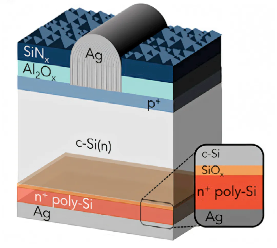
Schematic diagram of the cross section of a TOPCon solar cell
As shown in the figure, TOPCon process is formed by embedding a thin insulating layer of silicon oxide (SiOx) between the c-Si silicon wafer and the highly doped Poly layer. This structure of polysilicon passivation contact can achieve the functions of surface passivation and charge carrier selection, which helps to improve the efficiency of solar cells.
Main steps of preparing the Poly layer
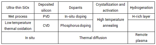
Main steps of preparing the Poly layer
Specific steps: Growth or deposition of thin film layer → deposition of silicon/silicon compound thin film → doping of dopants into silicon film → recrystallization of silicon and activation of dopants → hydrogenation
In the step of growing or depositing thin film layer, SiOₓ is usually chemically generated by immersing the silicon wafer in hot nitric acid at about 90°C to form a self-limited film of about 1.4nm, or by thermal oxidation in oxygen at 550°C - 700°C for a short time (about 10 minutes) to grow a film of about 2nm.
The technical process parameters in this step, such as deposition time, deposition rate, etc., will directly determine the thickness of the Poly layer.
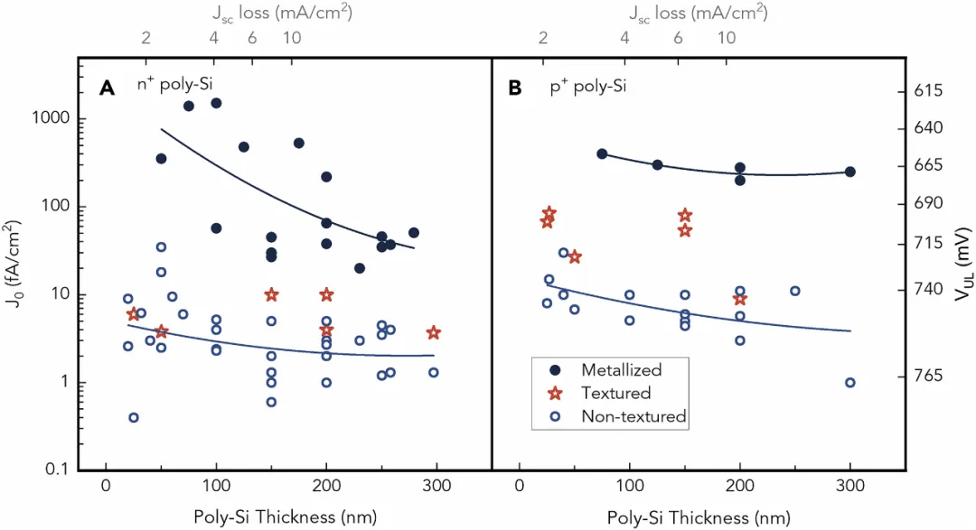
Poly layers formed by different preparation methods
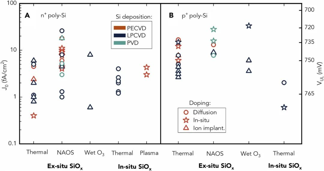
Poly layers formed by different preparation methods
As shown in the figure, it shows the influence of different interface oxide layer preparation technologies on the recombination current density (J0) and upper limit voltage (Vul) of n+Poly layer and p+Poly layer.
Recombination current density (J0): The lower J0 is, the smaller the recombination loss of the Poly layer is, and the better the battery performance is. The figure shows the influence of different interface oxide layer preparation technologies (such as thermal oxidation, nitric acid oxidation, ozone water oxidation, plasma oxidation) on J0.
Upper limit voltage (Vul): Vul is a theoretical value, which indicates the maximum open circuit voltage that the cell can reach when no recombination occurs. The higher Vul is, the greater the theoretical efficiency potential of the battery.
By reasonably controlling the interface layer and selecting the appropriate preparation technology, a Poly layer with low recombination current density can be achieved, which provides an important basis for improving the performance of solar cells.
Effect of Poly layer thickness on TOPCon cell performance
Effect of Poly Layer Thickness on Recombination and Current Loss
The figure shows the composite current density (left axis) and upper voltage (right axis) of the n+Poly layer and p+Poly layer as a function of the thickness of the Poly layer. The thickness of the deposited Poly layer has a significant impact on the junction performance.
Photon absorption loss: Absorption of photons in polysilicon leads to recombination losses. The absorption coefficient of doped polysilicon is similar to that of crystalline silicon. When the Poly layer is located on the front of the solar cell, each 10nm of polysilicon will cause a short-circuit current density loss of about 0.4 - 0.5mA/cm².
Infrared photon absorption: Free charge carriers present in the Poly layer absorb infrared photons. This loss also occurs when the Poly layer is located on the back of the cell. For a 140nm thick Poly layer, it will cause a loss of about 0.3 - 0.5mA/cm² (depending on the doping situation).
In TOPCon cells, the thickness of the Poly layer affects the absorption of photons. Too thick a Poly layer will increase the absorption of photons, thereby reducing the short-circuit current density. Therefore, the thickness of the Poly layer needs to be optimized to reduce optical loss, and the thickness of the Poly layer will directly affect the cell efficiency of TOPCon.
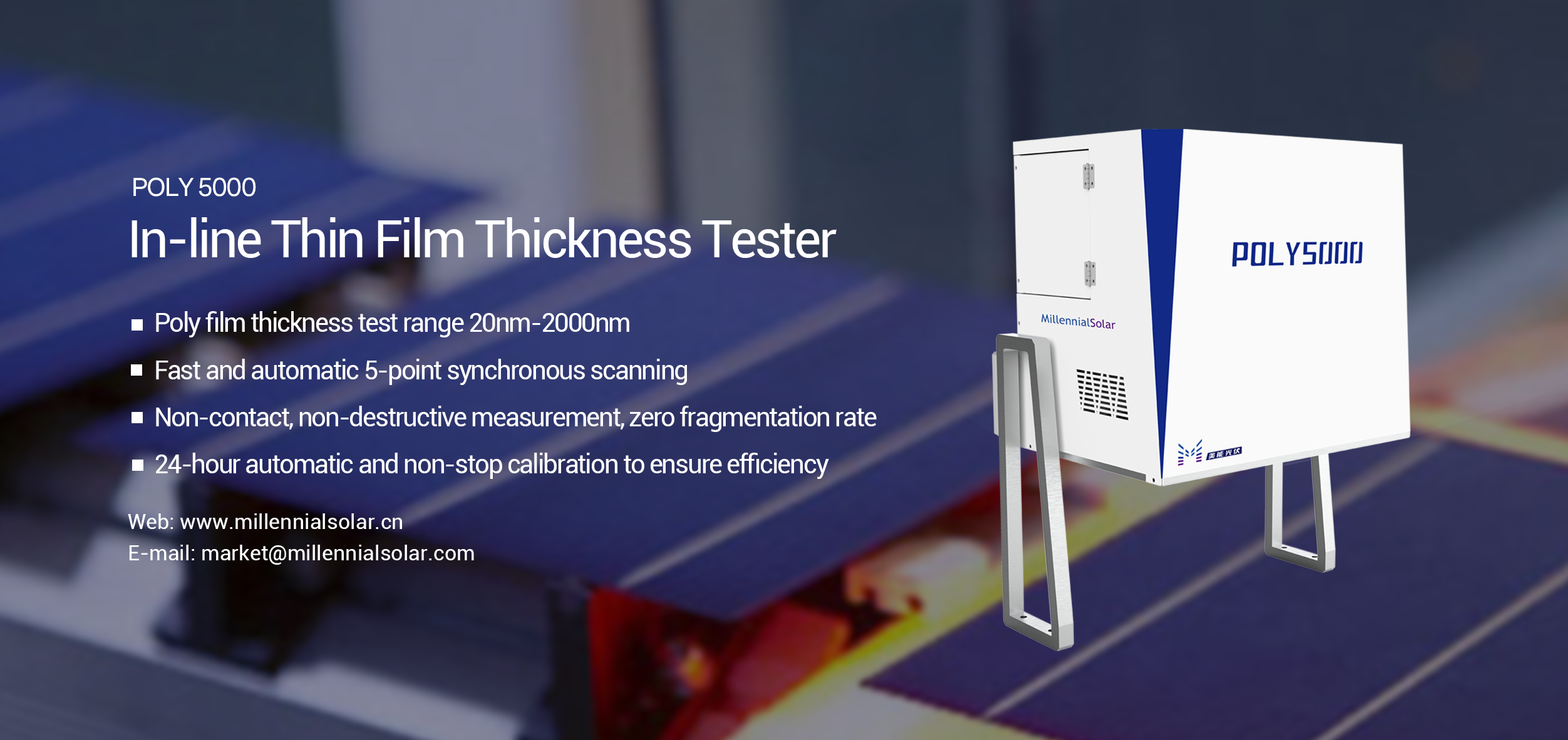
In-line Thin Film Thickness Tester
E-mail: market@millennialsolar.com
In-line Thin Film Thickness Tester can accurately detect the film thickness, and enable battery manufacturers to use the equipment for large-scale systematic testing in the deposition process production line, thereby helping cell manufacturers to greatly save testing time, improve production efficiency and quality assurance!
·Poly film thickness test range 20nm-2000nm
·Fast and automatic 5-point synchronous scanning
·Non-contact, non-destructive measurement, zero fragmentation rate
·24-hour automatic and non-stop calibration to ensure production efficiency
Poly layer thickness is an important factor affecting the performance of TOPCon solar cells. Its impact on photon absorption, short-circuit current, composite current density, etc. needs to be comprehensively considered in cell design and manufacturing to optimize cell performance. In-line Thin Film Thickness Tester is specially designed for photovoltaic process monitoring, helping customers to accurately obtain film thickness distribution information at different locations of samples, monitor process stability in real time, and thus optimize film thickness.


