
Quantum Efficiency Tester
PL/EL Integrated System
PV-Reflectumeter
3D Confocal Microscope
In-Line Four Point Probe Tester
Four Point Probe Tester
In-Line Thin Film Thickness Tester
Raman Spectrometer
FTIR Spectrometer
Spectrophotometer
Automatic Spectroscopic Ellipsometer
Contact Resistance Tester
Ultra depth of field 3D microscope
Auto Visual Tester
VMM PV Vision Measuring Machine
Solar Cell Horizontal Tensile Tester
Steady State Solar Simulator for Solar Cell
Solar Cell UV Aging Test Chamber
Solar Cell Comprehensive Tensile Tester
Visual Inspection Tester
Wet Leakage Current Tester
PV Module EL Tester
PV Module UV Preconditioning Chamber
Steady State Solar Simulator for PV Module
Current Continuous Monitor
Potential Induced Degradation Test
Bypass Diode Tester
LeTID Test System
Reverse Current Overload Tester
Impulse Voltage Tester
Hipot Insulation Tester
Ground Continuity Tester
Hipot Insulation Ground Tester
Damp Heat Test Chamber
Humidity Freeze Test
Thermal Cycle Test Chamber
Dynamic Mechanical Load Tester
Static Mechanical Load Tester
Hail Impact Tester
Robustness of Termination Tester
Module Breakage Tester
Cut Susceptibility Tester
Peel Shear Strength Tester
Universal Testing Machine (Single-arm)
Universal Testing Machine (Double-arm)
Glass Transmittance Tester
Acetic Acid Test Chamber
EVA Degree of Crosslinking Test System
Junction Box Comprehensive Tester
Drop ball tester
Semi-automatic scanning four-probe tester
Stylus Profilometer
Maximum Power Point Tracker
Perovskite Glass Transmittance Tester
Perovskite P1 Laser Scribing Multifunctional Testing Machine
Perovskite Online PL Tester
Perovskite Online Sheet Resistance Tester
Online Perovskite Film Thickness Tester
Perovskite Process Inspection Workstation
Portable EL Tester
Portable Thermal Imaging Tester
Solar Module Multi-Channel Testing System
PV Inverter Power Quality Tester
Drone EL Tester
IV Tester
IVEL Cell Sorting Machine
Deep Physical Mechanisms of Intrinsic Polycrystalline Silicon Insertion Layers in TOPCon Cells
Date : 3 February 2026Views : 1460
Tunnel-Oxidized Passivated Contact (TOPCon) technology has emerged as the mainstream high-efficiency crystalline silicon solar cell technology following PERC. Its core lies in the carrier-selective contact formed by an ultra-thin SiO₂ tunnel layer and a phosphorus-doped polycrystalline silicon (n-poly-Si) layer. However, the traditional uniformly heavily-doped poly-Si layer inherently conflicts with achieving both excellent passivation and low contact resistance. In recent years, an advanced structure—inserting an intrinsic poly-Si (i-poly-Si) layer within a gradient-doped n-poly-Si layer—has ingeniously resolved this contradiction at its physical core, propelling TOPCon performance to new heights. This paper systematically analyzes the underlying principles of this structure from the perspectives of semiconductor physics, band engineering, and carrier transport dynamics.
I. Physical Challenges of Conventional Uniformly Doped TOPCon
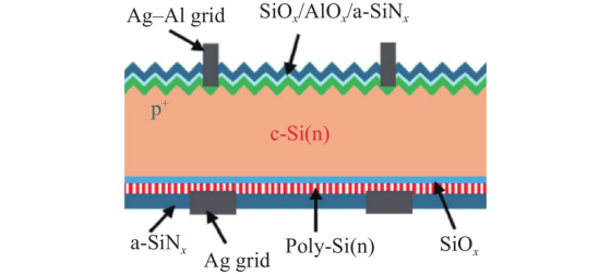
Schematic Diagram of TOPCon Cell Structure
To understand the necessity of the i-poly-Si insertion layer, we must first clarify the core challenges of the traditional TOPCon structure.
1. The Trade-off Between Passivation and Doping Concentration
The superior passivation of TOPCon stems from two mechanisms: chemical passivation of c-Si surface dangling bonds by an ultrathin SiO₂ layer, and field-effect passivation induced by the work function difference between n-poly-Si and c-Si. The latter requires sufficiently high doping concentration in the poly-Si layer to generate a strong built-in electric field. This field repels minority carriers (holes) from the c-Si surface, thereby suppressing surface recombination.
Contradiction: While excessively high doping concentrations enhance field-effect passivation, they also introduce two adverse effects:
• Reduced activation rate and carrier recombination: During high-temperature annealing to form polysilicon, excess phosphorus atoms cannot be fully activated, forming inactive phosphorus-silicon clusters or precipitates. These defects become strong centers for Shockley-Read-Hall (SRH) recombination, significantly increasing intrinsic recombination within the polysilicon layer.
• Parasitic absorption: High free carrier concentrations enhance the poly-Si layer's absorption of infrared light—known as parasitic absorption—reducing the cell's quantum efficiency in the long-wavelength spectrum.
2. The Conflict Between Contact Resistance and Poly-Si Quality
Ideal ohmic contacts require low barrier heights and thin depletion zones between metal and semiconductor. For poly-Si contacts, this necessitates high surface doping concentrations to reduce contact resistivity (ρc).
Conflict: As previously noted, overall high doping degrades poly-Si quality. While subsequent etching or laser doping can create localized heavy-doped regions at the surface, this increases process complexity and uncertainty.
II. Synergistic Mechanism of Gradient Doping and i-poly-Si Insertion Layer
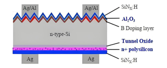
TOPcon Cell Process
The structure incorporating gradient doping and i-poly-Si insertion (typically: c-Si/SiO₂/i-poly-Si/n⁻-poly-Si/n⁺-poly-Si) represents not a simple layering but a meticulously designed synergy between band structure and defects.
1. The “Defect Filtering” and “Recrystallization Buffer” Functions of the Intrinsic Layer
• Physical Concept: During polycrystalline silicon recrystallization, defect generation (e.g., grain boundaries, dislocations, inactive dopant clusters) is closely correlated with dopant concentration. Highly doped regions serve as hotbeds for defect nucleation and growth.
• Function of the i-poly-Si layer:
Low-defect density zone: The intrinsic layer, free from lattice disturbances caused by foreign dopants, forms higher-quality, lower-defect-density polycrystalline silicon structures during crystallization. This directly creates a “highway” region with low recombination rates, where the probability of photogenerated carriers being captured and recombined by defects during transport is significantly reduced.
Isolating heavily doped defects: The i-poly-Si layer physically isolates the c-Si/SiO₂ interface from the heavily doped n⁺-poly-Si layer above. This means that even if the upper n⁺ layer contains a large number of recombination centers introduced by high phosphorus concentration, the “influence” of these centers on minority carriers at the c-Si interface is significantly weakened by the i-poly-Si layer. It acts as a “filter” or “insulating layer” for recombination defects.
2. Band Engineering “Soft Landing” and Field Effect Optimization
• “Cliff-like” Band Bending in Traditional Structures: In direct structures combining c-Si with uniformly heavily-doped n⁺-poly-Si, the band structure undergoes abrupt bending on both sides of the SiO₂, forming a high and narrow potential barrier. Although electrons can tunnel through, this process is highly sensitive to SiO₂ thickness and quality, and the strong built-in electric field also leads to high interfacial state excitation.
• “Gradient-like” Band Bending after i-poly-Si Insertion:
• Establishing an Internal Electric Field Gradient: This structure creates a gradual doping profile from c-Si to n⁺-poly-Si (c-Si → i-poly-Si → n⁻-poly-Si → n⁺-poly-Si). This corresponds to a gradual band bending rather than an abrupt transition.
• “Guiding” effect for majority carriers (electrons): For electrons (majority carriers), this gradual band structure resembles a smooth slope, guiding their transport from the c-Si base toward the metal electrode. While tunneling remains the primary mechanism for crossing SiO₂, once entering the poly-Si layer, their transport resembles drift motion within a quasi-neutral region guided by an electric field, encountering lower resistance.
The “High Wall” Effect for Minority Carriers (Holes): For holes (minority carriers), the presence of the i-poly-Si layer, interacting with the entire gradient-doped structure, forms a wider, more stable high barrier (a significant difference in valence band energy levels) on the c-Si surface side. This barrier effectively blocks hole diffusion toward the poly-Si side. More importantly, due to the low defect density of the i-poly-Si layer itself, even if holes approach this region through thermal motion, they lack effective recombination pathways. This makes the field-effect passivation effect not only strong but also extremely stable.
3. Maximizing Carrier Selectivity in Contacts
At its core, TOPCon is a high-performance electron-selective contact. The i-poly-Si insertion layer pushes this “selectivity” to its ultimate limit through the following mechanisms:
Exceptionally high electron selectivity (Se): This structure simultaneously optimizes handling capabilities for both charge carriers.
For electrons: Provides low-resistance tunneling and drift paths (high conductivity).
For holes: Provides strong blocking and near-zero recombination rates (high resistivity, low recombination). This dual optimization results in an extremely electron-selective contact region, manifested as exceptionally low contact resistivity and extremely high open-circuit voltage (Voc).
III. Theoretical Summary and Outlook
The insertion of intrinsic poly-Si within the gradient-doped poly-Si layer of TOPCon cells represents an ingenious design rooted in profound physical insight. Its core principles can be summarized as follows:
Spatial Decoupling: Decoupling the spatially coupled functions of “bulk passivation quality” and “contact conductivity.” The i-poly-Si/n⁻-poly-Si layer ensures high-quality bulk passivation and carrier guidance, while the surface n⁺-poly-Si layer is dedicated to achieving low contact resistance.
Band Modulation: By constructing a doping gradient, it enables a “soft landing” of the band structure, optimizing majority carrier transport while enhancing blocking for minority carriers.
Defect Engineering: Utilizing the i-poly-Si layer as a low-defect “buffer zone” effectively isolates the c-Si-sensitive interface from the highly doped region with high defect density, suppressing SRH recombination at its source.
This structure not only significantly enhances the Voc and efficiency limits of TOPCon cells but also demonstrates the decisive role of synergistic bandgap and defect design at the microscopic scale in modern semiconductor devices.


