
Quantum Efficiency Tester
PL/EL Integrated System
PV-Reflectumeter
3D Confocal Microscope
In-Line Four Point Probe Tester
Four Point Probe Tester
In-Line Thin Film Thickness Tester
Raman Spectrometer
FTIR Spectrometer
Spectrophotometer
Automatic Spectroscopic Ellipsometer
Contact Resistance Tester
Ultra depth of field 3D microscope
Auto Visual Tester
VMM PV Vision Measuring Machine
Solar Cell Horizontal Tensile Tester
Steady State Solar Simulator for Solar Cell
Solar Cell UV Aging Test Chamber
Solar Cell Comprehensive Tensile Tester
Visual Inspection Tester
Wet Leakage Current Tester
PV Module EL Tester
PV Module UV Preconditioning Chamber
Steady State Solar Simulator for PV Module
Current Continuous Monitor
Potential Induced Degradation Test
Bypass Diode Tester
LeTID Test System
Reverse Current Overload Tester
Impulse Voltage Tester
Hipot Insulation Tester
Ground Continuity Tester
Hipot Insulation Ground Tester
Damp Heat Test Chamber
Humidity Freeze Test
Thermal Cycle Test Chamber
Dynamic Mechanical Load Tester
Static Mechanical Load Tester
Hail Impact Tester
Robustness of Termination Tester
Module Breakage Tester
Cut Susceptibility Tester
Peel Shear Strength Tester
Universal Testing Machine (Single-arm)
Universal Testing Machine (Double-arm)
Glass Transmittance Tester
Acetic Acid Test Chamber
EVA Degree of Crosslinking Test System
Junction Box Comprehensive Tester
Drop ball tester
Semi-automatic scanning four-probe tester
Stylus Profilometer
Maximum Power Point Tracker
Perovskite Glass Transmittance Tester
Perovskite P1 Laser Scribing Multifunctional Testing Machine
Perovskite Online PL Tester
Perovskite Online Sheet Resistance Tester
Online Perovskite Film Thickness Tester
Perovskite Process Inspection Workstation
Portable EL Tester
Portable Thermal Imaging Tester
Solar Module Multi-Channel Testing System
PV Inverter Power Quality Tester
Drone EL Tester
IV Tester
IVEL Cell Sorting Machine
Poly-Si Finger Structure: An Analysis of the Physical Mechanisms and Performance Limits of Contact Microstructures
Date : 27 March 2026Views : 895
Tunneling Oxide Passivated Contact (TOPCon) technology has emerged as the mainstream technology route for high-efficiency crystalline silicon solar cells following PERC. Its core lies in a composite layer consisting of ultra-thin silicon dioxide (SiO₂) and doped polycrystalline silicon (poly-Si), which replaces the heavily doped region found in traditional cells. Within this framework, the “poly-Si finger” structure—formed by patterning the poly-Si layer—is a key design element for enabling front- or back-side metallization and approaching the theoretical efficiency limit. This paper analyzes the physical mechanisms of the poly-Si finger from the perspectives of quantum tunneling, carrier selectivity, and optical and electrical losses.
I. Evolution of Contact Structures: From Localized Contacts to Global Passivated Contacts
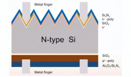
Schematic Diagram of Poly-finger Technology for TOPCon Cells
In traditional PERC or Al-BSF cells, the metal electrode makes direct contact with the silicon substrate. To suppress minority carrier recombination in the contact region, heavy doping is required beneath the contact point to form an emitter or back field. However, localized heavy doping introduces issues such as Auger recombination enhancement, band narrowing, and parasitic absorption.
TOPCon technology achieves a global passivated contact structure, with the basic composition being: c-Si / SiOₓ (approximately 1–2 nm) / n⁺-poly-Si (or p⁺-poly-Si). In this structure, the ultra-thin SiOₓ layer achieves chemical passivation through saturated silicon dangling bonds, significantly reducing the surface recombination rate; while the doped poly-Si layer induces an intrinsic electric field at the SiOₓ/Si interface, repelling minority carriers and efficiently collecting majority carriers. Poly-Si fingers are selectively windowed based on this structure to achieve low-resistance connection with metal electrodes while maintaining passivation performance.
II. Physical Mechanisms and Performance Control of Poly-Si Fingers
Polysilicon finger structure
Quantum Tunneling and Carrier-Selective Transport
An ultra-thin SiOₓ layer forms a triangular potential barrier for majority carriers, enabling transport via Fowler-Nordheim tunneling under an electric field. This process exhibits carrier selectivity: the barrier shape is determined by the work function difference between the poly-Si and the silicon substrate, as well as the doping type, allowing majority carriers to tunnel effectively while blocking minority carriers. This selectivity is preserved in the poly-Si finger region, ensuring efficient charge collection and low recombination at the metal contacts.
Microscopic Sources of Contact Resistivity
Current is conducted from the metal electrodes through the poly-Si fingers, and the contact resistivity (ρc) is determined by two factors. First is the contact between the metal and heavily doped poly-Si, which can form a good ohmic contact, with ρc reaching the order of 0.1 mΩ·cm². Second is the tunneling process of carriers through the SiOₓ layer between the poly-Si and the silicon substrate, whose resistance is influenced by the thickness, mass, and interface state density of the oxide layer. Therefore, the design of poly-Si fingers must strike a balance between low contact resistivity and high passivation mass.
Trade-off Between Optical and Electrical Losses
When the TOPCon structure is used on the front side of the cell, poly-Si fingers introduce shading losses. Narrower fingers with smaller spacing can shorten the lateral carrier transport distance, reduce lateral resistance losses at the emitter, and improve the fill factor; wider fingers with larger spacing, on the other hand, reduce the shading area and increase the short-circuit current. Unlike metal grid lines, poly-Si fingers, being semiconductor materials, introduce their own sheet resistance as an additional source of series resistance. Therefore, optimization requires a comprehensive consideration of the trade-off among the lateral resistance of the emitter, the longitudinal resistance of the fingers, and shading losses.
Localization Characteristics of Recombination Losses
Ideally, recombination centers exist only in the areas covered by metal electrodes—that is, the localized regions where poly-Si fingers contact the silicon substrate. Due to the passivation properties of TOPCon, these recombination regions are confined to discrete contact points, while the rest of the cell remains in a low-recombination state, thereby bringing the open-circuit voltage close to the theoretical limit of silicon material.
III. Key Issues in the Fabrication Process
Regarding doping methods, in-situ doping allows dopant sources to be introduced simultaneously with polysilicon deposition, resulting in good interface quality; however, it poses challenges in terms of uniformity and concentration control. Ion implantation combined with annealing enables precise dose control, but high-energy ions may damage the ultra-thin SiO₃ layer, and subsequent high-temperature annealing may cause dopant diffusion and polysilicon recrystallization.
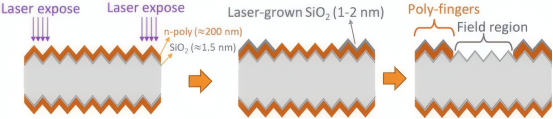
Regarding patterning techniques, photolithography and etching offer high precision and are suitable for the laboratory fabrication of ultra-fine finger-like structures (<10 µm), but they are relatively costly; laser windowing or doping can achieve one-step patterning, but damage to the SiO₂ layer and silicon substrate caused by the laser must be controlled; printing combined with etching is a viable solution for industrialization, requiring a balance between precision and cost.
IV. Future Technical Directions
Further research on poly-Si fingers points toward next-generation cell technologies. Gridless and copper plating technologies can be integrated with poly-Si fingers to reduce shading and improve conductivity. In back-contact cells, the poly-Si fingers for the positive and negative electrodes are arranged in an interlaced pattern on the back of the cell, completely eliminating front-side shading. This approach can achieve conversion efficiencies exceeding 26%, placing higher demands on the doping precision, isolation performance, and passivation quality of the fingers. Additionally, the poly-Si/SiO₂/c-Si structure in TOPCon inherently possesses carrier selectivity, which can be extended to complex structures such as silicon-based tandem cells.
The poly-Si finger structure in TOPCon cells integrates quantum tunneling, field-effect passivation, carrier selectivity, low-resistance contacts, and optical management. A deep understanding of its physical mechanisms is fundamental to optimizing cell performance, overcoming efficiency bottlenecks, and driving the development of next-generation cell technologies.


