


Non-contact IV tester

Quantum Efficiency Tester
Accurate EQE, IQE and spectral response measurements—from localized spots to full cells.
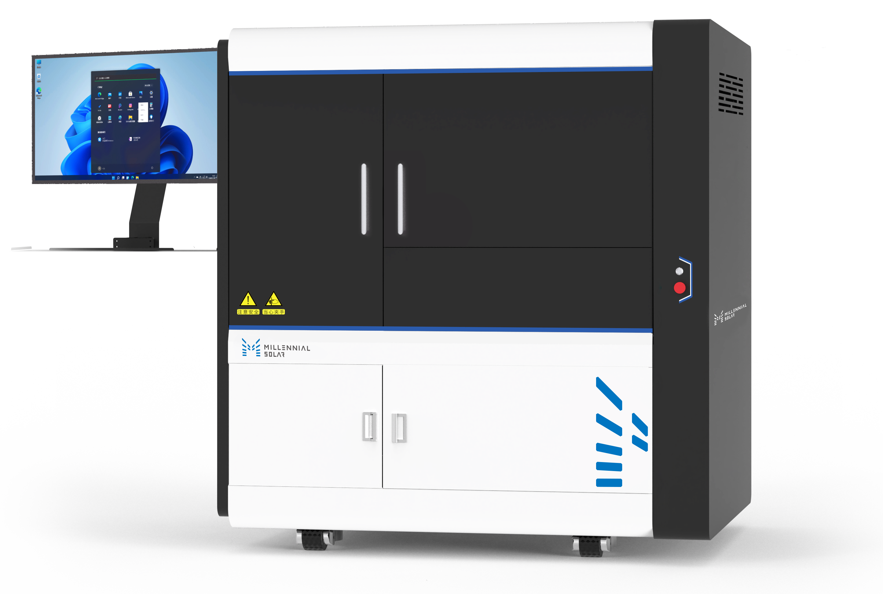
The MNPVQE-1800T PRO is designed for photovoltaic research and production, providing accurate measurements of solar cell spectral response, external quantum efficiency (EQE/IPCE) and internal quantum efficiency (IQE). The MNPVQE-1800T PRO supports a wide range of photovoltaic devices, including crystalline silicon, multicrystalline silicon, amorphous silicon, microcrystalline silicon, CdTe, CIGS, CIS, Ge, dye-sensitized, organic/polymer, tandem, multijunction, quantum-well, quantum-dot, chalcogenide and perovskite solar cells.PL/EL Integrated System
PV-Reflectumeter
3D Confocal Microscope
In-Line Four Point Probe Tester
Four Point Probe Tester
In-Line Thin Film Thickness Tester
Raman Spectrometer
FTIR Spectrometer
Spectrophotometer
Automatic Spectroscopic Ellipsometer
Contact Resistance Tester
Ultra depth of field 3D microscope
Auto Visual Tester
VMM PV Vision Measuring Machine
Solar Cell Horizontal Tensile Tester
Steady State Solar Simulator for Solar Cell
Solar Cell UV Aging Test Chamber
Solar Cell Comprehensive Tensile Tester
Visual Inspection Tester
Wet Leakage Current Tester
PV Module EL Tester
PV Module UV Preconditioning Chamber
Steady State Solar Simulator for PV Module
Current Continuous Monitor
Potential Induced Degradation Test
Bypass Diode Tester
LeTID Test System
Reverse Current Overload Tester
Impulse Voltage Tester
Hipot Insulation Tester
Ground Continuity Tester
Hipot Insulation Ground Tester
Damp Heat Test Chamber
Humidity Freeze Test
Thermal Cycle Test Chamber
Dynamic Mechanical Load Tester
Static Mechanical Load Tester
Hail Impact Tester
Robustness of Termination Tester
Module Breakage Tester
Cut Susceptibility Tester
Peel Shear Strength Tester
Universal Testing Machine (Single-arm)
Universal Testing Machine (Double-arm)
Glass Transmittance Tester
Acetic Acid Test Chamber
EVA Degree of Crosslinking Test System
Junction Box Comprehensive Tester
Drop ball tester
Semi-automatic scanning four-probe tester
Stylus Profilometer
Maximum Power Point Tracker
Perovskite Glass Transmittance Tester
Perovskite P1 Laser Scribing Multifunctional Testing Machine
Perovskite Online PL Tester
Perovskite Online Sheet Resistance Tester
Online Perovskite Film Thickness Tester
Perovskite Process Inspection Workstation
Portable EL Tester
Portable Thermal Imaging Tester
Solar Module Multi-Channel Testing System
PV Inverter Power Quality Tester
IV Tester
IVEL Cell Sorting Machine
24.3%-Efficient Perovskite/Silicon Tandem Solar Cells Fabricated by an All-Vacuum Process
Date : 6 November 2026Views : 40
Industrializing perovskite photovoltaics requires materials and processes that combine high efficiency, high throughput, and low cost. All-vacuum processing has attracted attention because it is solvent-free, enables uniform large-area coating, and can conformally cover textured silicon bottom cells. However, conventional vacuum evaporation has low deposition rates, particularly for organic components, creating a major throughput bottleneck. Close-space sublimation (CSS) reduces the distance between source and substrate, allowing rapid sublimation of organic precursors at relatively high pressure, with high material utilization and deposition rates.
This study systematically investigated CSS for fabricating wide-bandgap perovskites and successfully applied it to efficient single-junction and tandem solar cells.
Millennial Solar QE tester can accurately measure solar-cell external quantum efficiency (EQE) and spectral response, supporting interface engineering and back-contact design optimization to improve quantum efficiency and overall cell performance.
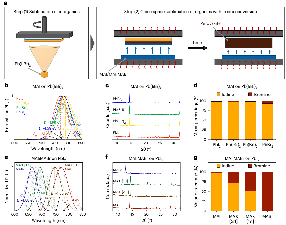
(a) Schematic of the two-step fabrication process for the perovskite absorber.(b) Photoluminescence (PL) spectra of perovskite films obtained by converting different inorganic frameworks using a pure MAI organic source for 35 minutes. Corresponding (c) XRD patterns and (d) iodine-to-bromine ratios measured by EDX. (e) PL spectra, (f) XRD patterns, and (g) iodine-to-bromine ratios measured by EDX for the corresponding perovskite films.
Bromine is generally required to prepare wide-bandgap perovskites. The study found that, in a two-step CSS process, converting bromine-containing inorganic frameworks (such as PbI₂/PbBr₂ mixtures) using a pure MAI organic source yielded films consisting almost entirely of MAPbI₃, regardless of the initial bromine fraction in the inorganic source. XRD and EDX analyses indicated extensive halide exchange during CSS: iodine from the organic source entered the solid phase, while bromine in the inorganic framework was displaced and volatilized as MABr. Thus, the final perovskite composition was governed primarily by the halide flux in the vapor phase rather than by the inorganic framework.
The researchers therefore introduced bromine exclusively through the organic source, using pure PbI₂ as the inorganic layer and MAI:MABr mixed powders with different mass ratios as the organic source. As the MABr fraction increased, the perovskite bandgap could be continuously tuned from 1.55 to 1.88 eV, accompanied by a linear increase in bromine content. EDX and XRD confirmed this trend. The mixed-halide organic source maintained a stable composition during prolonged use without selective depletion, demonstrating reusability and reliable composition control. Adjusting the MAI:MABr ratio therefore enables precise, stable control of the CSS-grown perovskite bandgap.
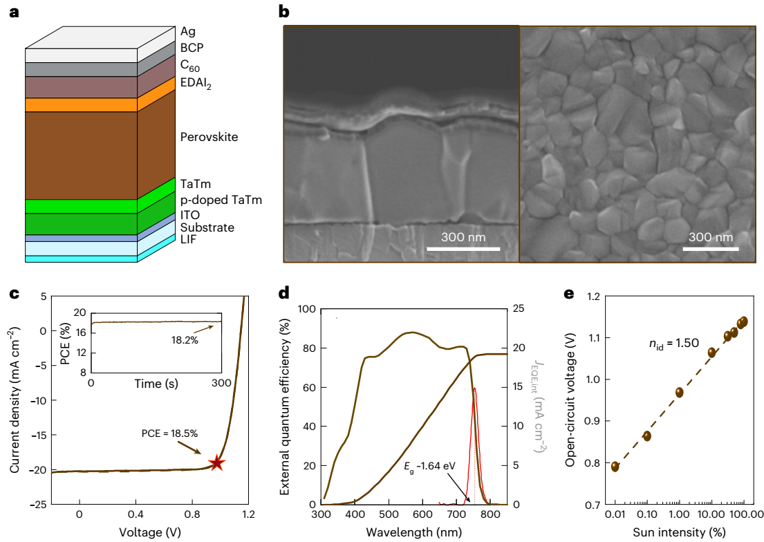
(a) Layer-stack schematic of an all-vacuum-processed p-i-n perovskite solar cell. (b) Cross-sectional SEM image and corresponding surface morphology of the perovskite absorber. (c) Current density–voltage (J–V) curve of the champion cell and stabilized power conversion efficiency under maximum power point tracking (MPPT). (d) External quantum efficiency (EQE) spectrum and corresponding integrated current density of the champion cell. (e) Light-intensity dependence of Voc for a passivated device under one-sun illumination.
Based on these findings, the researchers used an MAI:MABr mass ratio of 3:1 to convert a PbI₂ layer into a MAPb(I₀.₈Br₀.₂)₃ absorber with a bandgap of 1.64 eV in just 10 minutes. With a p-i-n device structure, an EDAI₂ surface-passivation layer, and a LiF antireflection layer, the champion cell achieved 18.5% power conversion efficiency (18.2% stabilized), an open-circuit voltage of 1.15 V, and a fill factor of 79.2%, with negligible hysteresis. The study reported this as the highest efficiency at the time for a purely MA-based wide-bandgap (>1.6 eV) perovskite cell fabricated entirely by vacuum processing. After 400 hours of aging under one-sun illumination at 65°C and 85°C, the devices retained more than 95% of their initial efficiency. A semitransparent device also achieved 16.2% efficiency, demonstrating potential for tandem applications.
Tandem Solar Cells: 24.3% Efficiency and Broad Process Compatibility
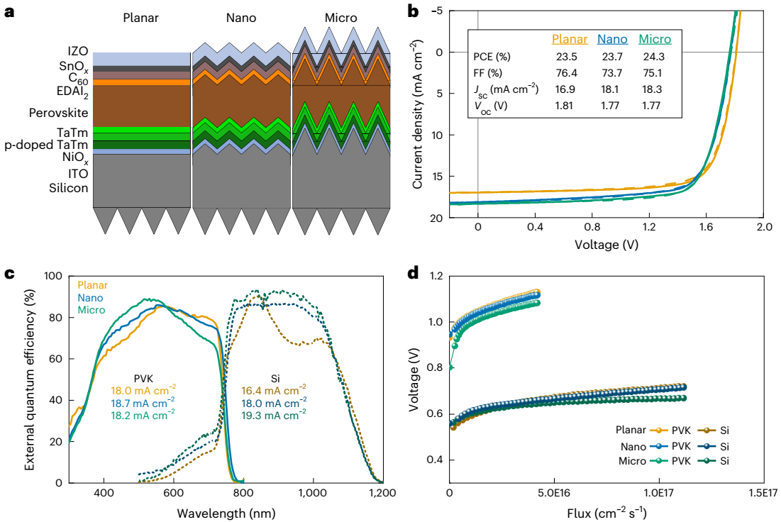
(a) Layer-stack schematics of two-terminal (2T) tandem cells using planar, nanotextured, and microtextured silicon bottom cells. (b) J–V curves of the champion tandem cells. (c) EQE spectra and corresponding integrated current densities of the perovskite top and silicon bottom cells for each configuration. (d) Light-intensity dependence of the perovskite top-cell voltage, measured by selective-illumination Suns–Voc, for each tandem configuration.
The researchers further integrated CSS-grown perovskite layers into monolithic 2T perovskite/silicon tandem cells using three silicon heterojunction bottom-cell morphologies: planar, nanotextured (submicrometer pyramids), and microtextured. Perovskite deposition parameters were identical across the three configurations; only charge-transport-layer thicknesses were adjusted to account for differences in surface area. Device performance was highly consistent, with open-circuit voltages of 1.77–1.81 V and fill factors of approximately 75%. Enhanced light trapping increased short-circuit current density to 18.1–18.3 mA/cm² in textured devices. The microtextured configuration achieved a champion efficiency of 24.3%, compared with 23.5% and 23.7% for planar and nanotextured cells, respectively. This was reported as one of the highest efficiencies for fully textured 2T tandem cells fabricated entirely by vacuum processing.
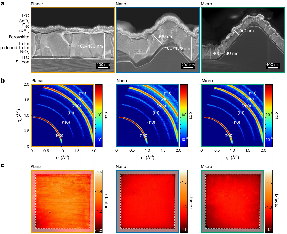
(a) Cross-sectional SEM images of complete tandem cells using planar, nanotextured, and microtextured silicon bottom cells. (b) GIWAXS patterns of the corresponding perovskite films. (c) Heat maps of perovskite-film uniformity obtained by PL intensity-dependent imaging (k-imaging), where the k factor reflects film quality.
EQE and selective-illumination Suns–Voc measurements showed that the perovskite top cells had consistent bandgaps (~1.66 eV), integrated current densities (18.0–18.7 mA/cm²), and voltage outputs (~1.09 V) across all three configurations. The silicon bottom-cell response improved with increasing texture. Cross-sectional SEM images showed conformal CSS coverage on all three surface morphologies, with similar perovskite grain sizes and columnar growth patterns. GIWAXS and PL imaging further confirmed nearly identical crystal orientation, crystallinity, and uniformity across the configurations.
This study demonstrates that CSS is an all-vacuum deposition technique combining high-throughput potential, high material utilization, and excellent process compatibility. It addresses the low deposition-rate limitation of conventional vacuum evaporation and accommodates different substrate morphologies and surface chemistries, producing wide-bandgap perovskite films with consistent photovoltaic properties on planar, nanotextured, and microtextured silicon bottom cells. The resulting devices achieved 18.5% single-junction efficiency and 24.3% tandem efficiency, indicating a practical all-vacuum pathway toward industrial perovskite photovoltaic manufacturing.
By adjusting the MAI:MABr ratio in the organic source, the perovskite bandgap was tuned from 1.55 to 1.88 eV. The vapor-phase halide supply, rather than the inorganic precursor composition, governed the final film composition.
Q2: What efficiencies were achieved using the all-vacuum CSS process?The champion wide-bandgap single-junction cell reached 18.5% efficiency (18.2% stabilized), while the microtextured perovskite/silicon tandem cell achieved 24.3%.
Q3: Can CSS be used on different silicon surface textures?Yes. CSS produced conformal perovskite films on planar, nanotextured, and microtextured silicon bottom cells, with tandem efficiencies of 23.5%, 23.7%, and 24.3%, respectively.
E-mail: market@millennialsolar.com
The Millennial Solar QE Quantum Efficiency Tester measures the spectral response of solar cells and uses quantum efficiency data to identify wavelength regions with reduced spectral response. Its advantages include broad solar-cell compatibility, a wide spectral measurement range, measurement accuracy, and traceability.
▶ Compatible with all types of solar cells to meet diverse testing requirements.
▶ Spectral range up to 300–2500 nm, with customization available.
▶ Dual xenon and halogen light sources for stable illumination.
Original Research Reference: Close-space sublimation as a versatile deposition process for efficient perovskite silicon tandem solar cells
Related Products


