


Non-contact IV tester

Quantum Efficiency Tester
PL/EL Integrated System
PV-Reflectumeter
3D Confocal Microscope
In-Line Four Point Probe Tester
Four Point Probe Tester
In-Line Thin Film Thickness Tester
Raman Spectrometer
FTIR Spectrometer
Spectrophotometer
Automatic Spectroscopic Ellipsometer
Contact Resistance Tester
Ultra depth of field 3D microscope
Auto Visual Tester
VMM PV Vision Measuring Machine
Solar Cell Horizontal Tensile Tester
Steady State Solar Simulator for Solar Cell
Solar Cell UV Aging Test Chamber
Solar Cell Comprehensive Tensile Tester
Visual Inspection Tester
Wet Leakage Current Tester
PV Module EL Tester
PV Module UV Preconditioning Chamber
Steady State Solar Simulator for PV Module
Current Continuous Monitor
Potential Induced Degradation Test
Bypass Diode Tester
LeTID Test System
Reverse Current Overload Tester
Impulse Voltage Tester
Hipot Insulation Tester
Ground Continuity Tester
Hipot Insulation Ground Tester
Damp Heat Test Chamber
Humidity Freeze Test
Thermal Cycle Test Chamber
Dynamic Mechanical Load Tester
Static Mechanical Load Tester
Hail Impact Tester
Robustness of Termination Tester
Module Breakage Tester
Cut Susceptibility Tester
Peel Shear Strength Tester
Universal Testing Machine (Single-arm)
Universal Testing Machine (Double-arm)
Glass Transmittance Tester
Acetic Acid Test Chamber
EVA Degree of Crosslinking Test System
Junction Box Comprehensive Tester
Drop ball tester
Semi-automatic scanning four-probe tester
Stylus Profilometer
Maximum Power Point Tracker
Perovskite Glass Transmittance Tester
Perovskite P1 Laser Scribing Multifunctional Testing Machine
Perovskite Online PL Tester
Perovskite Online Sheet Resistance Tester
Online Perovskite Film Thickness Tester
Perovskite Process Inspection Workstation
Portable EL Tester
Portable Thermal Imaging Tester
Solar Module Multi-Channel Testing System
PV Inverter Power Quality Tester
IV Tester
IVEL Cell Sorting Machine
BC Cell IV Characteristics: Comparative Evaluation of Contact and Non-Contact Measurement
Date : 23 September 2026Views : 70
In interdigitated back-contact (IBC) solar cells, both the positive and negative electrodes are located on the rear side. Conventional contact-based IV testing therefore faces challenges such as complex contact design, potential cell damage, and lengthy measurement times, making it particularly unsuitable for in-line inspection in production. To address these challenges, a photoluminescence-based non-contact measurement method has been developed. By measuring the reflectance spectrum, multi-wavelength luminescence signals, and locally shadowed images, the external quantum efficiency (EQE) can be reconstructed using optical models. Suns-PL is then used to obtain a pseudo I-V curve, and the voltage drop caused by series resistance is subtracted to generate the complete I-V characteristics. Because the method requires no physical contact throughout the measurement process, it can avoid electrode damage, significantly reduce testing time, and support process monitoring.
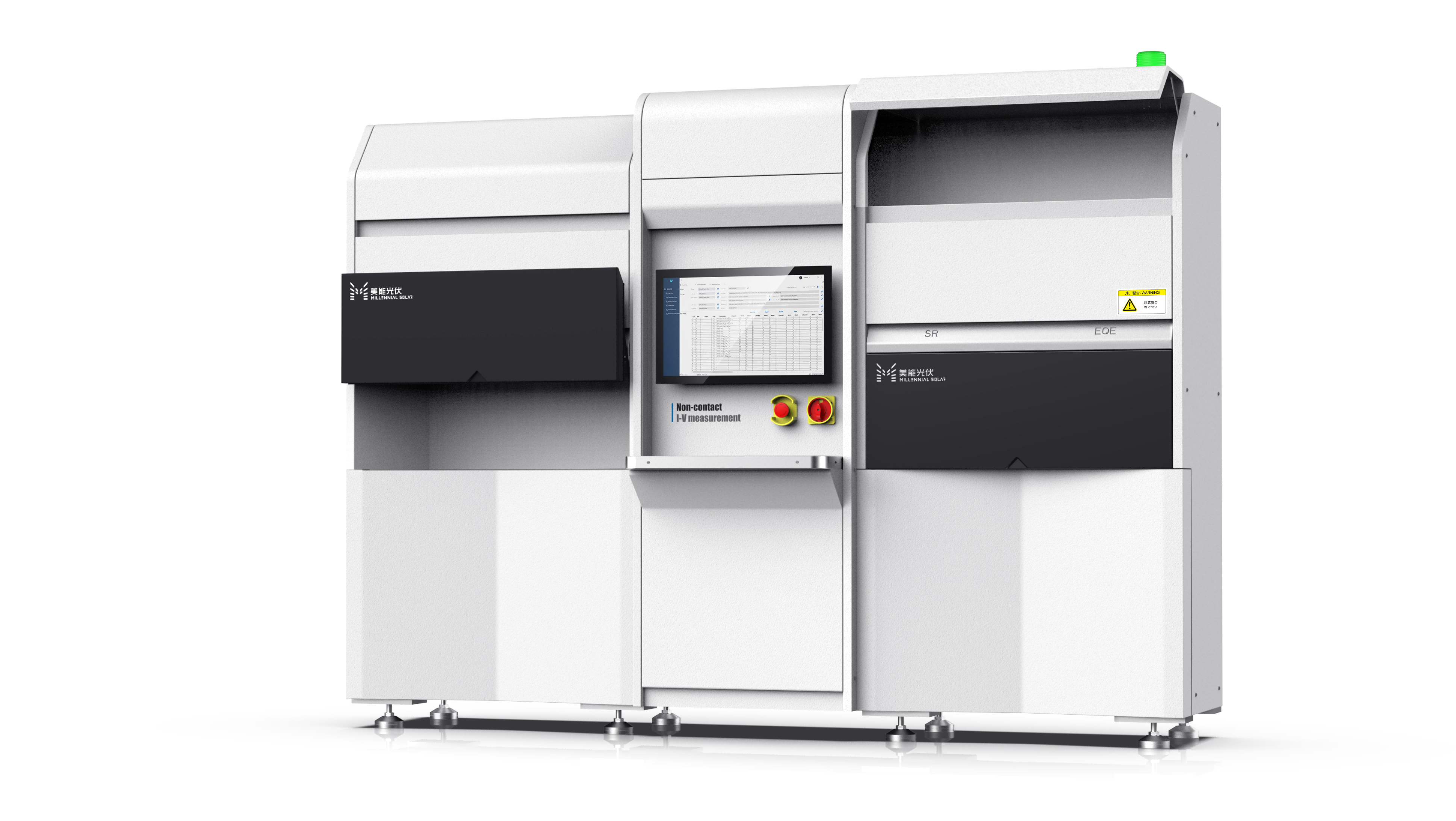
Millennial Solar Non-contact IV tester provides non-destructive, consumable-free, millisecond-level measurement for BC and busbar-free cells, with simultaneous acquisition of multiple parameters including IV, EQE, and PL.
This study systematically applies the method to industrial-grade M10-size IBC cells. By cross-comparing the results with those obtained using a standard contact-based flash tester, the study evaluates measurement accuracy and reliability for key parameters including open-circuit voltage, short-circuit current, series resistance, and efficiency. Pixel-level series-resistance imaging is also used to reveal the lateral resistance distribution within the cells, providing a basis for subsequent process optimization and practical implementation of the method.
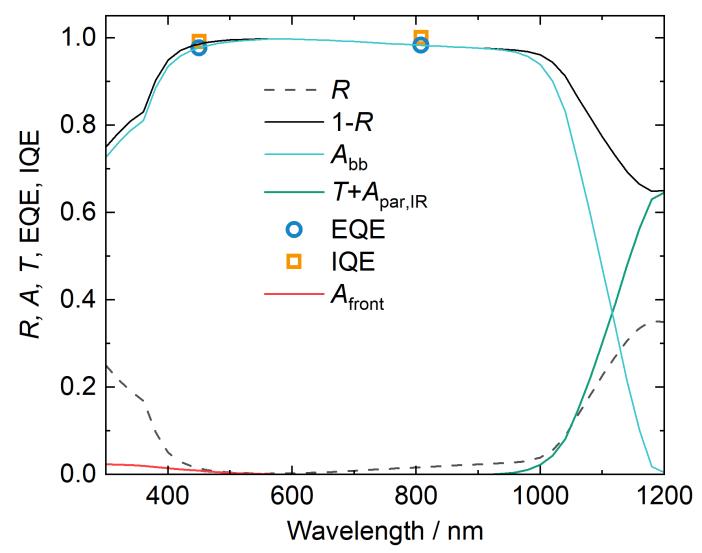
To determine the carrier generation rate Abb, the measured reflectance spectrum R and relative EQE measured at 450 nm and 808 nm are combined with an optical model for light trapping, escape light and transmission T, and parasitic absorption in the infrared range Apar,IR, as well as a model for front-film parasitic absorption Afront in the UV and blue spectral ranges.
The essence of the non-contact method is to “measure electrical characteristics optically.” The core process is as follows:
1. First, the cell's reflectance spectrum and photoluminescence signals at two specific wavelengths, 450 nm and 808 nm, are measured. Combined with optical models, including the Lambertian light-trapping model and parasitic absorption models, these measurements are used to reconstruct the absolute external quantum efficiency (EQE) over a broad spectral range of 300–1200 nm. The short-circuit current density Jsc is then calculated from the reconstructed EQE.
2. Second, Suns-PL is used to measure photoluminescence intensity under different illumination levels and calibrate the measurements to open-circuit voltage, producing a “pseudo IV curve” without the influence of series resistance.
3. Third, the photoluminescence images obtained under uniform illumination and local shadow illumination are compared to quantitatively calculate the series resistance Rs and its planar distribution. The calculation can be performed on a pixel-by-pixel basis to generate a resistance distribution map.
4. Finally, the voltage drop caused by series resistance is subtracted from the pseudo IV curve to reconstruct the actual I-V characteristics, from which key parameters such as fill factor and efficiency can be obtained.
The study selected 150 finished M10-size IBC cells, classified into low, medium, and high-quality groups according to their factory quality grades. Each cell was tested using both the above non-contact method and the standard contact-based flash tester used on the production line, enabling direct comparison of the results.
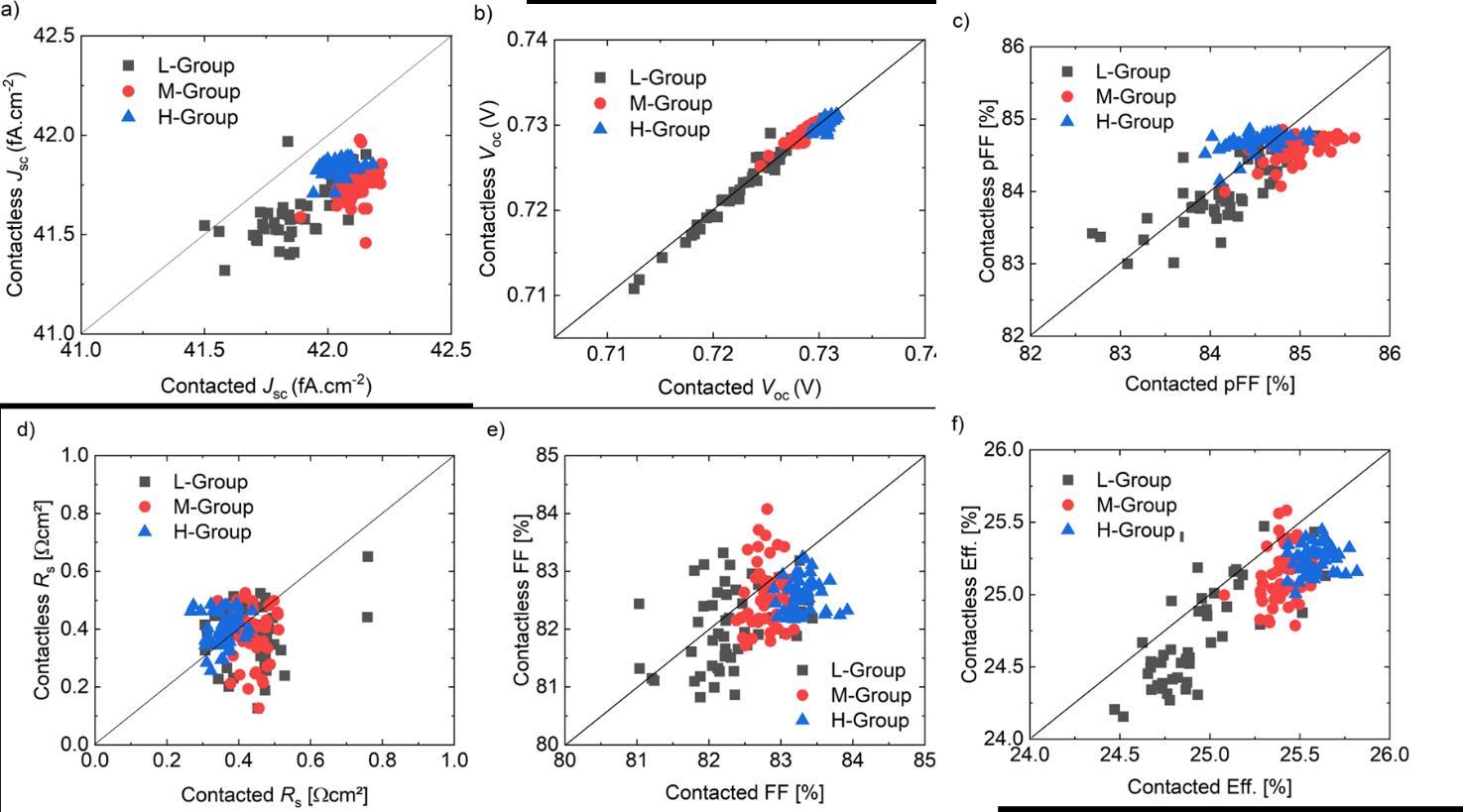
Comparison of Performance Parameters Measured by Contact and Non-Contact Methods
Comparison of the two measurement methods showed the following:
Short-circuit current density (Jsc): The overall trends were consistent (R = 0.64), but two differences were observed. First, the non-contact results were approximately 0.25 mA/cm² lower; possible causes include flash-tester calibration or the simplified EQE approach. Second, the contact-based Jsc of the medium-quality group was higher than that of the high-quality group, whereas the non-contact results showed the opposite trend.
Open-circuit voltage (Voc): The two methods showed close agreement over the range of 712–733 mV, with an RMSE of only 0.7 mV and R = 0.98. Among all parameters, Voc showed the closest agreement.
Pseudo fill factor (pFF): The trends were reasonably close (R = 0.71), with an absolute RMSE of 0.37 percentage points. However, the contact-based pFF of the medium-quality group was higher than that of the high-quality group, while the non-contact results were similar between the two groups. The contact-based pFF of the high-quality group showed greater dispersion, which may be related to hysteresis effects; this group also had the highest open-circuit voltage and the strongest hysteresis.
Series resistance (Rs): The average values were in agreement, but the data showed substantial scatter (R = 0.03). The Rs distribution maps showed increased resistance at the two ends of the busbars, along the upper and lower edges of the silicon wafer, and along the cut edges of half cells. In the central region, the current-collection path through the busbar was approximately half the pad-to-pad distance, whereas it could be about twice as long near the edges. The longer current path naturally increases resistance. This indicates that there is room to optimize pad placement, which may help reduce resistance losses and improve module power.
Fill factor and efficiency: The correlation was R = 0.78, with the deviation mainly attributable to differences in Jsc. The non-contact FF and efficiency of the high-quality group were slightly lower, primarily because the non-contact Rs was somewhat higher for this group.
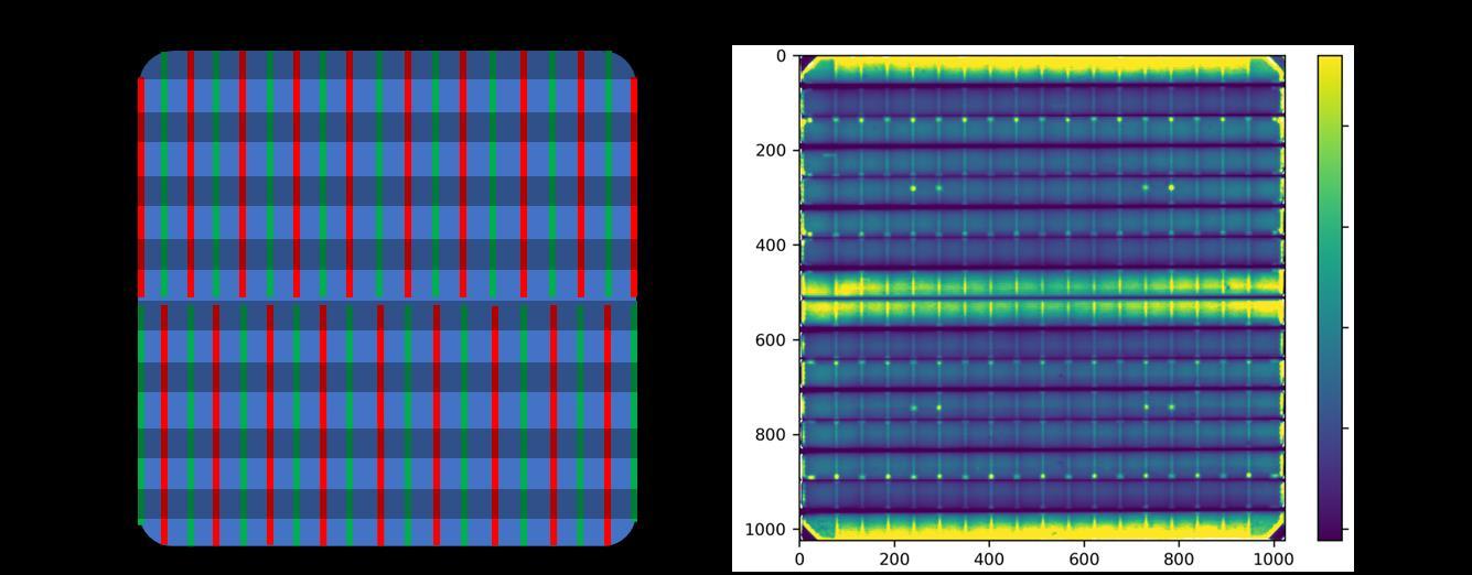
a) Schematic of the partial-shadow PL imaging setup;
b) Rs distribution image of one sample measured using the non-contact shadow-mask method.
The distinctive value of the non-contact method lies in its imaging capability. The resulting Rs distribution map clearly shows significantly increased series resistance at the ends of the busbars and along the cut edges of half cells. This is consistent with physical expectations because current in these regions must travel a longer distance through the fine gridlines before reaching the busbar, naturally increasing resistance. This information directly indicates a potential optimization direction: improving the layout of pads (or busbar connection points) to reduce resistive losses and improve efficiency.
This study successfully applied a non-contact IV measurement method to industrial-grade IBC solar cells. The results show that the method can obtain key performance parameters with relatively high accuracy, with particularly reliable measurements of open-circuit voltage. Some systematic deviation or data scatter remains in the measurements of Jsc and Rs, but these issues may be improved through more refined calibration and automated testing platforms. The value of the method lies not only in its non-contact nature, which avoids contact-induced damage and complex fixture design, but also in its ability to provide spatially resolved information such as planar series-resistance distribution, offering a useful analytical tool for optimizing cell and module performance. With its speed, non-destructive operation, and rich information output, the method has broad potential for future research characterization, particularly for in-line inspection in production environments.
The non-contact method measures reflectance spectra and photoluminescence (PL) at selected wavelengths to reconstruct the external quantum efficiency (EQE) and calculate Jsc. Suns-PL is then used to obtain a pseudo I-V curve, while series-resistance correction generates the final I-V characteristics.
Q2: How accurate is non-contact I-V measurement for IBC solar cells?The method shows strong agreement with conventional contact-based testing, particularly for open-circuit voltage (Voc). For M10-size IBC cells, Voc measurements achieved an R value of 0.98 with an RMSE of only 0.7 mV.
Q3: What are the advantages of non-contact I-V measurement for BC cells?Non-contact I-V measurement requires no physical contact, helping avoid electrode damage and complex contact fixtures. It also provides spatially resolved series-resistance data, making it useful for process optimization and in-line inspection of BC solar cells.
E-mail: market@millennialsolar.com
With years of experience in photovoltaic testing, Millennial Solar combines mass-production experience with advances in academic research to provide a millisecond-level, non-destructive testing solution for crystalline-silicon solar cells across production lines.
· Millisecond-level measurement: Eliminates time-consuming mechanical movements, matches high-speed production lines, and enables substantially higher throughput.
· Zero physical contact: Suitable for advanced structures such as ultra-thin wafers, busbar-free cells, and BC cells, with no physical damage and no consumables.
· Broad compatibility: PERC / TOPCon / HJT / BC and more.
· Five-dimensional data acquisition: IV + EQE + SR + Re + PL.
Millennial Solar's non-contact IV tester sets a new approach to high-efficiency solar cell testing. Zero physical contact eliminates the risks of microcracks and contamination caused by physical contact, while millisecond-level throughput is designed to match production-line takt time. High-precision measurement data provide a reliable basis for process optimization while reducing maintenance and consumable costs. This enables high-efficiency cell production to pursue both quality and testing efficiency without the need for the same trade-off between them.
Original reference: Contactless Measurement of Current-Voltage Characteristics of Back-Contact Solar Cells


