


Non-contact IV tester

Quantum Efficiency Tester
Accurate EQE, IQE and spectral response measurements—from localized spots to full cells.
The MNPVQE-1800T PRO is designed for photovoltaic research and production, providing accurate measurements of solar cell spectral response, external quantum efficiency (EQE/IPCE) and internal quantum efficiency (IQE). The MNPVQE-1800T PRO supports a wide range of photovoltaic devices, including crystalline silicon, multicrystalline silicon, amorphous silicon, microcrystalline silicon, CdTe, CIGS, CIS, Ge, dye-sensitized, organic/polymer, tandem, multijunction, quantum-well, quantum-dot, chalcogenide and perovskite solar cells.PL/EL Integrated System
PV-Reflectumeter
3D Confocal Microscope
In-Line Four Point Probe Tester
Four Point Probe Tester
In-Line Thin Film Thickness Tester
Raman Spectrometer
FTIR Spectrometer
Spectrophotometer
Automatic Spectroscopic Ellipsometer
Contact Resistance Tester
Ultra depth of field 3D microscope
Auto Visual Tester
VMM PV Vision Measuring Machine
Solar Cell Horizontal Tensile Tester
Steady State Solar Simulator for Solar Cell
Solar Cell UV Aging Test Chamber
Solar Cell Comprehensive Tensile Tester
Visual Inspection Tester
Wet Leakage Current Tester
PV Module EL Tester
PV Module UV Preconditioning Chamber
Steady State Solar Simulator for PV Module
Current Continuous Monitor
Potential Induced Degradation Test
Bypass Diode Tester
LeTID Test System
Reverse Current Overload Tester
Impulse Voltage Tester
Hipot Insulation Tester
Ground Continuity Tester
Hipot Insulation Ground Tester
Damp Heat Test Chamber
Humidity Freeze Test
Thermal Cycle Test Chamber
Dynamic Mechanical Load Tester
Static Mechanical Load Tester
Hail Impact Tester
Robustness of Termination Tester
Module Breakage Tester
Cut Susceptibility Tester
Peel Shear Strength Tester
Universal Testing Machine (Single-arm)
Universal Testing Machine (Double-arm)
Glass Transmittance Tester
Acetic Acid Test Chamber
EVA Degree of Crosslinking Test System
Junction Box Comprehensive Tester
Drop ball tester
Semi-automatic scanning four-probe tester
Stylus Profilometer
Maximum Power Point Tracker
Perovskite Glass Transmittance Tester
Perovskite P1 Laser Scribing Multifunctional Testing Machine
Perovskite Online PL Tester
Perovskite Online Sheet Resistance Tester
Online Perovskite Film Thickness Tester
Perovskite Process Inspection Workstation
Portable EL Tester
Portable Thermal Imaging Tester
Solar Module Multi-Channel Testing System
PV Inverter Power Quality Tester
IV Tester
IVEL Cell Sorting Machine
Converting PERC Production Lines to p-IBC: Optimizing Aluminum Paste Silicon Content and Peak Firing Temperature to Reduce Metallization Recombination
Date : 11 November 2026Views : 20
Existing PERC production lines can be converted to p-type interdigitated back-contact (p-IBC) solar-cell production. The p-type base uses the aluminum-based metallization established in PERC manufacturing, while the n-type polycrystalline silicon (n-polySi) emitter uses silver-paste contacts from TOPCon technology. This enables substantial equipment reuse and a lower thermal budget than the boron-diffusion process of standard TOPCon cells. The trade-off is the large rear-side metallized area: recombination at the metal–semiconductor interface can significantly reduce open-circuit voltage (Voc). Quokka3 simulations identified aluminum metallization as the principal efficiency bottleneck for p-IBC cells, adversely affecting both Voc and fill factor (FF). A study using M2-size gallium-doped p-type Czochralski silicon wafers optimized aluminum-paste silicon content and peak firing temperature, reducing metallization-induced implied open-circuit voltage (iVoc) loss to approximately 5 mV while achieving specific contact resistivity below 1 mΩ·cm² and a champion cell efficiency of 23.3%.
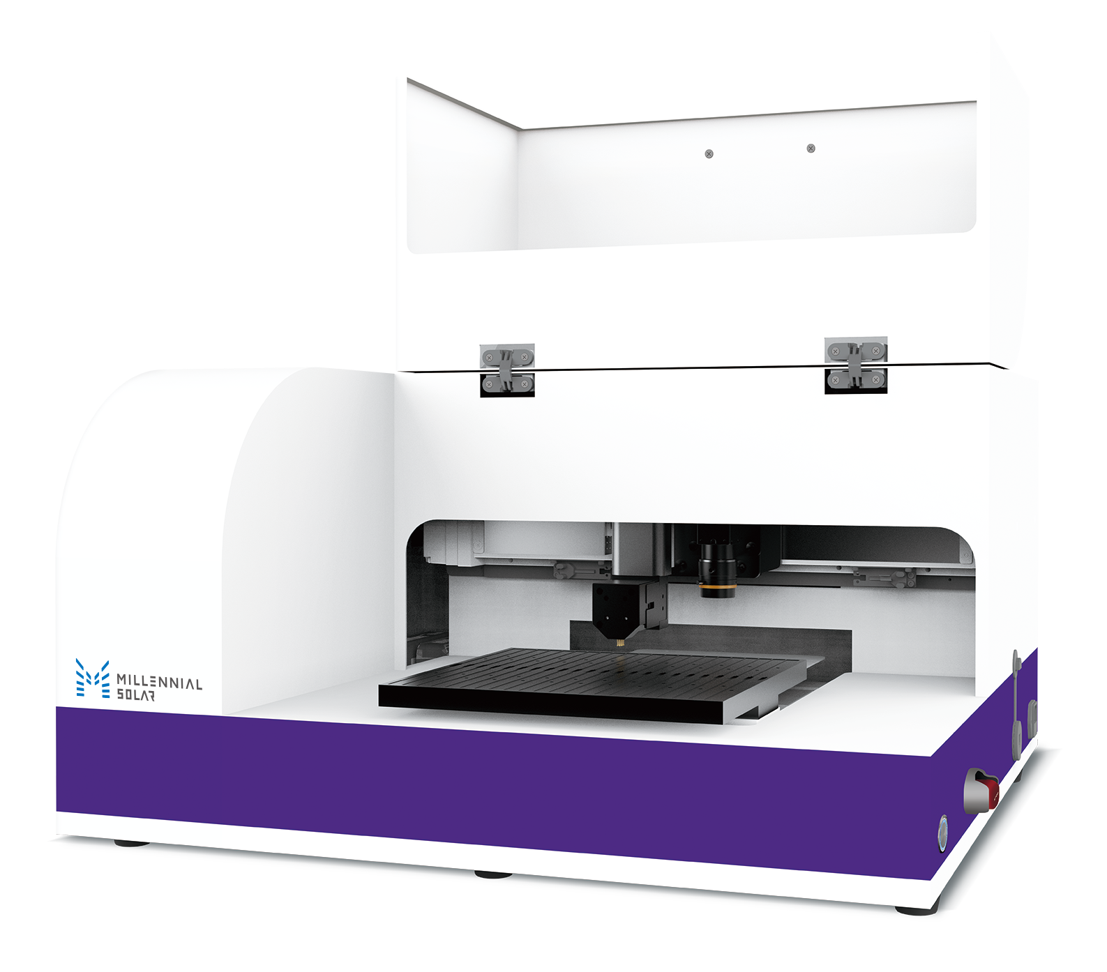
Millennial Solar TLM Contact Resistance Tester is a high-precision instrument for extracting key electrical parameters in solar-cell electrode optimization, supporting both specific contact resistivity and gridline resistance measurements.

Cross-section of a p-IBC solar cell: front-side texturing on a Ga-doped p-type silicon substrate; a rear tunnel oxide and n-type poly-Si layer; an AlOx/SiNy passivation stack; aluminum-based contacts to the base and silver-based contacts to the emitter, arranged as interdigitated fingers.
Commercial M2-size Ga-doped p-type Czochralski silicon wafers with resistivity of 1–2 Ω·cm were used. SiOx was deposited on the front by PECVD as a masking layer, followed by alkaline texturing to form random pyramids, while the rear surface remained polished. Wet-chemical cleaning followed. A thin interfacial oxide was thermally grown on the rear, and in-situ phosphorus-doped amorphous silicon was deposited by PECVD using silane and phosphine. Subsequent thermal annealing in an oxygen-containing atmosphere crystallized the n-polySi and simultaneously formed a protective front-side masking layer.
The interdigitated rear base and emitter patterns were defined by nanosecond green-laser ablation, followed by wet alkaline cleaning to remove laser damage and an oxidizing wet-chemical clean. The passivation stack comprised ALD-deposited AlOx and PECVD-deposited SiNy on both sides. ALD was performed through alternating cycles in a tube furnace: oxygen was dissociated by radio-frequency plasma in the first step, and trimethylaluminum was introduced thermally at approximately 300°C in the second. After opening the base-region dielectric with a nanosecond green laser, aluminum paste was printed to form contacts in a process similar to PERC rear-side contacting. Silver paste was screen-printed on the emitter regions, followed by co-firing at a peak temperature of approximately 800°C.
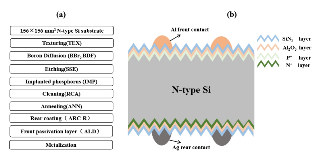
(a) Manufacturing process. (b) Schematic structure of an N-PERT solar cell.
Process optimization followed two approaches. First, aluminum-paste silicon content was divided into four levels (Low, Medium, High, and Very high) and combined with three peak firing temperatures (T−15°C, T, and T+15°C) to form a two-dimensional process matrix. Second, n-polySi thickness was varied at three levels (High, Medium, and Low), and cell characteristics were measured by I–V testing.
Contact resistance was measured on dedicated test structures using the transmission line method (TLM). iVoc loss was determined by photoluminescence (PL) imaging: because QSSPC cannot be performed directly on metallized regions, the relationship between area-averaged PL intensity and iVoc was first calibrated using QSSPC on non-metallized regions. This calibration was then applied to PL images of metallized regions to calculate their area-averaged iVoc. The difference between the iVoc of non-metallized and metallized regions on the same wafer was taken as the loss.
Contact resistance increased as aluminum-paste silicon content increased and peak firing temperature decreased, showing a consistent trend. A low-silicon aluminum paste combined with a suitable firing temperature achieved specific contact resistivity below 1 mΩ·cm² and widened the usable firing window. The study reported only the upper bound of “below 1,” without an exact value or uncertainty.
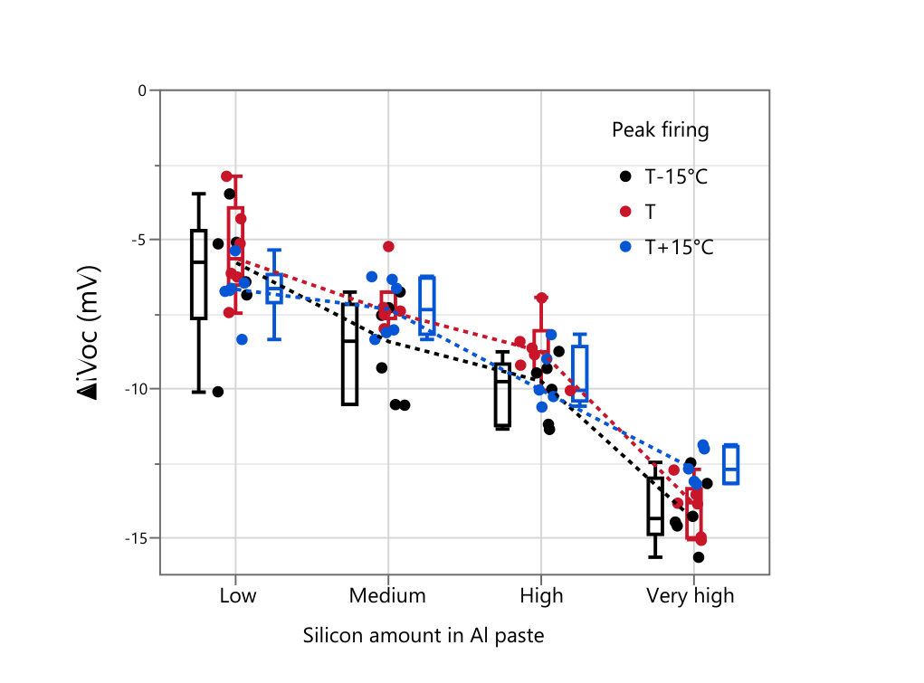
Box plots of metallization-induced iVoc loss versus aluminum-paste silicon content, grouped by peak firing temperature (T−15°C, T, and T+15°C). The vertical axis is ΔVoc (mV), where negative values indicate loss. Loss increases with silicon content and can be reduced to approximately 5 mV.
Metallization-induced iVoc loss followed the opposite trend: lower silicon content resulted in lower loss. The study explicitly noted that this contradicted earlier findings suggesting a beneficial role for silicon content in aluminum-alloy metallization. In the p-IBC base-region aluminum contacts studied here, the trend was reversed. The study did not explain the cause or provide cross-validation. Fine-tuning the peak firing temperature reduced iVoc loss to approximately 5 mV, again without a reported uncertainty.
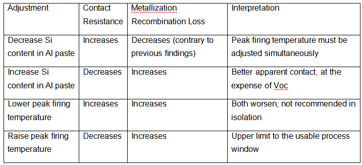
The two variables therefore cannot be optimized independently. Lowering silicon content increases contact resistance, so peak firing temperature must be adjusted to recover a viable process window. Lowering peak firing temperature alone worsens both contact resistance and recombination loss. Raising it reduces contact resistance but increases recombination loss, placing an upper limit on the process window.
The effects and trade-offs of both variables are summarized below:
PL imaging provides visual evidence consistent with these findings. In symmetric samples with different metallization fractions, the silver-contact patterns on n-polySi were almost invisible in PL images, indicating good contact passivation. Before optimization, the aluminum-metallized p-type base regions showed markedly lower PL intensity; after optimization, the metallized regions became brighter and the contrast with non-metallized regions decreased. The three panels are not a single matched comparison: the left panel shows silver contacts on n-polySi, whereas the center and right panels compare the p-type base before and after optimization. The study described these observations qualitatively and did not provide numerical PL intensities.
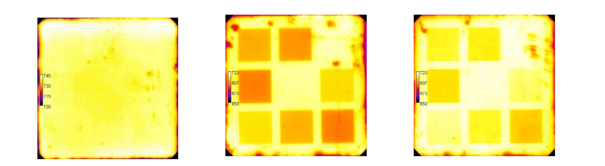
Three PL images: left, symmetric samples with different metallization densities on n-polySi; center, p-type base before optimization; right, p-type base after optimization. PL intensity increases in the metallized regions after optimization.
Thinning the n-polySi layer yielded a 0.1 mA·cm⁻² gain in Jsc through reduced free-carrier absorption, but Voc deteriorated. The study stated that further investigation was needed to determine whether the voltage decrease was related to metallization, and speculated that paste penetration through the tunnel oxide might be involved. This remains an unverified hypothesis. The Jsc gain did not translate into an efficiency improvement in this study.
A specially designed asymmetric test structure replaced the conventional IBC stripe-ablation pattern with large-area laser-ablated regions to enable QSSPC measurements. The iVoc of non-metallized test regions ranged from 730 to 740 mV, with the base and n-polySi regions at the lower and upper ends, respectively. Another passage in the study reported 733 mV, which is not fully consistent with the range given in the abstract. The champion cell achieved Jsc of 40.6 mA·cm⁻², Voc of 720 mV, FF of 79.8%, and efficiency of 23.3%. The difference between the iVoc of the non-metallized precursor and the Voc of the champion cell represents the voltage penalty associated with metallization and contacting. The efficiency was measured in the laboratory; the study did not state whether it was independently certified.
For rear aluminum metallization when converting a PERC line to p-IBC, aluminum-paste silicon content and peak firing temperature must be adjusted together. Reducing silicon content helps lower metallization recombination loss but increases contact resistance, requiring temperature adjustment to restore a viable process window. A practical sequence is to test lower silicon-content levels, then sweep peak firing temperature to identify the lowest temperature at which specific contact resistivity remains around or below 1 mΩ·cm². The study achieved approximately 5 mV iVoc loss, specific contact resistivity below 1 mΩ·cm², and a champion cell efficiency of 23.3%.
The observed relationship between silicon content and recombination loss runs counter to earlier studies and is a particularly important parameter not to transfer uncritically during line conversion. The PERC-era assumption that higher silicon content is more robust came from silver–aluminum paste systems; this study found the opposite trend for the p-IBC configuration. It documented the trend without investigating the underlying mechanism.
The limitations are equally important. Neither the approximately 5 mV loss nor the below-1 mΩ·cm² contact resistivity was accompanied by an uncertainty estimate or a more precise value. The four-by-three silicon-content/temperature matrix was tested only for the aluminum paste used in this study; the optimum may shift with a different paste. The reversed trend lacks a mechanistic explanation and should not be assumed to hold for other paste systems.
Related evidence offers context but cannot be transferred directly across cell structures. In another study, firing-through aluminum paste was applied to an n-type silicon cell with a boron-diffused emitter. The front local-contact specific resistivity was 1.0 mΩ·cm², the dark saturation current density beneath the metal contact (J0,metal) was 61% lower than with silver–aluminum paste, and the pseudo-efficiency measured by Suns–Voc was 21.34%, compared with 21.00% for silver–aluminum paste. These results show that aluminum paste can reduce metal-contact recombination, consistent in broad terms with the p-IBC findings. However, a boron emitter on an n-type substrate is not the same contact configuration as an aluminum contact to the p-type base of a p-IBC cell, so the numerical results cannot be directly transferred.
A production-relevant failure mode associated with IBC rear metallization also warrants attention. The rear metallization effectively divides the cell electrically into several weakly coupled subcells, with tree-like branch connections between solder pads. Interconnection mismatch can short the polarities or leave approximately one-third of the cell open-circuited. Electroluminescence (EL) testing identified such connection faults at currents as low as 1 A with a 0.5 s exposure, enabling automated screening through simple image processing before encapsulation.
However, 1 A is well below the normal operating condition described in the study (approximately 6 A near short circuit). It establishes a demonstrated detection threshold, not a recommended production-line test setting.
In the tested paste system, lower silicon content reduced metallization-related iVoc loss but increased contact resistance. Peak firing temperature therefore had to be optimized alongside silicon content.
Q2: What performance was achieved after metallization optimization?The study reported approximately 5 mV iVoc loss, specific contact resistivity below 1 mΩ·cm², and a champion p-IBC cell efficiency of 23.3%.
Q3: Can the optimized firing conditions be applied directly to other aluminum pastes?Not necessarily. The reported trends were established for one aluminum-paste system, and the study did not explain the mechanism behind the reversed silicon-content trend.
E-mail: market@millennialsolar.com
Millennial Solar TLM Contact Resistance Tester enables fast, flexible, and precise specific contact resistivity measurements.
Static measurement repeatability ≤1%; dynamic measurement repeatability ≤3%.
●Line resistance measurement accuracy: 5% or 0.1 Ω/cm.
●Switch freely between specific contact resistivity and line resistance measurements.
●Customizable probe heads for different measurement and analysis needs.
Original Research References: Development of a p-type Silicon Interdigitated Back Contact Solar Cell With Passivated Contacts; Low Recombination Firing-Through Al Paste for N-Type Solar Cell with Boron Emitter; Well Intended Contact Failures on Interdigitated Back Contact Solar Cells.
Disclaimer: Original and reposted articles published by the Millennial Solar WeChat official account are intended solely for academic exchange and sharing information related to the photovoltaic industry. Unauthorized plagiarism, alteration, quotation, or republication that infringes upon the account’s rights is prohibited. The content is provided for reference only. If any infringement is identified, please contact us for removal.
Related Products


