
Quantum Efficiency Tester
PL/EL Integrated System
PV-Reflectumeter
3D Confocal Microscope
In-Line Four Point Probe Tester
Four Point Probe Tester
In-Line Thin Film Thickness Tester
Raman Spectrometer
FTIR Spectrometer
Spectrophotometer
Automatic Spectroscopic Ellipsometer
Contact Resistance Tester
Ultra depth of field 3D microscope
Auto Visual Tester
VMM PV Vision Measuring Machine
Solar Cell Horizontal Tensile Tester
Steady State Solar Simulator for Solar Cell
Solar Cell UV Aging Test Chamber
Solar Cell Comprehensive Tensile Tester
Visual Inspection Tester
Wet Leakage Current Tester
PV Module EL Tester
PV Module UV Preconditioning Chamber
Steady State Solar Simulator for PV Module
Current Continuous Monitor
Potential Induced Degradation Test
Bypass Diode Tester
LeTID Test System
Reverse Current Overload Tester
Impulse Voltage Tester
Hipot Insulation Tester
Ground Continuity Tester
Hipot Insulation Ground Tester
Damp Heat Test Chamber
Humidity Freeze Test
Thermal Cycle Test Chamber
Dynamic Mechanical Load Tester
Static Mechanical Load Tester
Hail Impact Tester
Robustness of Termination Tester
Module Breakage Tester
Cut Susceptibility Tester
Peel Shear Strength Tester
Universal Testing Machine (Single-arm)
Universal Testing Machine (Double-arm)
Glass Transmittance Tester
Acetic Acid Test Chamber
EVA Degree of Crosslinking Test System
Junction Box Comprehensive Tester
Drop ball tester
Semi-automatic scanning four-probe tester
Stylus Profilometer
Maximum Power Point Tracker
Perovskite Glass Transmittance Tester
Perovskite P1 Laser Scribing Multifunctional Testing Machine
Perovskite Online PL Tester
Perovskite Online Sheet Resistance Tester
Online Perovskite Film Thickness Tester
Perovskite Process Inspection Workstation
Portable EL Tester
Portable Thermal Imaging Tester
Solar Module Multi-Channel Testing System
PV Inverter Power Quality Tester
Drone EL Tester
IV Tester
IVEL Cell Sorting Machine
Introduction to Photoluminescence Imaging (PLI) Technology
Date : 29 June 2026Views : 25
Photoluminescence Imaging (PLI) is a non-contact, high-spatial-resolution optical characterization technique that reveals key information about semiconductor materials and devices—such as carrier recombination, defect distribution, and interface quality—by recording the spatial distribution of photoluminescence intensity on the material surface. The following is a comprehensive analysis of its principles, system configuration, and typical applications:
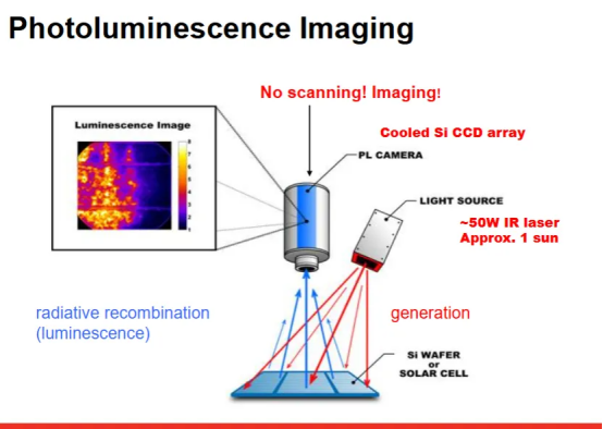
How Does PL Imaging Work? 1. Excitation-Emission Process:· Excitation: A laser or LED light source (typically selected at a wavelength near the material’s absorption edge) illuminates the sample surface, exciting photo-generated carriers (EHP) following an interband transition.
· Diffusion and Recombination: Carrier diffusion leads to recombination at defects or junction regions, where radiative recombination emits photons (photon wavelength ≈ bandgap; e.g., Si ≈ 1150 nm, perovskite ≈ 800 nm).
· Signal Acquisition: A high-sensitivity camera (e.g., InGaAs, CCD) captures the luminescence intensity distribution → forming a two-dimensional PL image.
2. Correlation between Signal Intensity and Recombination:· Areas of high PL intensity: High radiative recombination efficiency → Few defects, good passivation.
· Areas with low PL intensity: Non-radiative recombination (SRH, surface recombination) dominates → defects or interface issues.
What components make up a PL imaging system?A complete PL (photoluminescence) imaging system typically consists of five major components: an excitation light source, an optical system, a detector, a motion stage, and data acquisition and analysis software. These modules work together to determine the system’s detection sensitivity, spatial resolution, and detection efficiency.
For industrial inspection, although configurations vary across different application scenarios (such as silicon wafer inspection, LED wafer inspection, and perovskite film inspection), the overall architecture remains largely consistent.
The following sections describe each component and its function.
Module
Function and Typical Parameters
Examples of Commercial Equipment
Excitation Light Source
- Laser wavelength: 405 nm (perovskite), 532 nm (Si), 785 nm (GaAs) - Power density: Adjustable from 0.1 to 1000 mW/cm²
Laser diode modules (Thorlabs), tunable lasers
Optical Lens Assemblies
- High-NA objectives achieve micrometer-level resolution (<10 μm) - Filters separate the excitation light from the PL signal
Nikon CFI S Plan Fluor objective
Detector
- InGaAs camera (sensitive to near-infrared, compatible with Si) - Back-illuminated CCD (visible light range, suitable for perovskites) - Cooled to -80°C to suppress dark current
Hamamatsu InGaAs camera, Andor iXon series CCD
Sample Stage and Translation Stage
- XYZ motorized translation stage, accuracy ±1 μm - Temperature control range: -190°C to 300°C (low-temperature PL imaging)
Thorlabs motorized stages, Linkam temperature-controlled stages
Software Analysis System
- Image stitching (wide-area scanning) - Intensity correction (field-flattening/dark-field subtraction) - Quantitative parameter extraction (lifetime, uniformity)
Custom LabVIEW Software, Pylon Viewer
Typical Application Scenarios for PL Imaging 1. Visualization of Defects and Grain Boundaries Case Study: Polycrystalline Silicon Solar Cells
Phenomenon: PL images show dark lines at grain boundaries (see illustration below) → Impurity enrichment (Fe, Cu, etc.) at grain boundaries leads to accelerated SRH recombination.
Quantitative Analysis: Analysis of grain boundary contrast () → If contrast > 30%, the impurity absorption process requires optimization. Ideal grain region: ▉▉▉ PL intensity: 1200 a.u.Grain Boundary Region: ▒▒▒ PL Intensity: 400 a.u. ⇒ ( )

2. Carrier Lifetime Imaging (Combined with TRPL) Method: Measure PL decay curves point by point → Extract local lifetimes τ(x,y) and image them. Software Algorithms: 3. Homogeneity Statistical Parameters Homogeneity Index (HU): σ is the standard deviation, and μ is the average intensity
HU > 95% is the standard for high performance
Challenges and SolutionsTechnical Challenges
Countermeasures
Low signal-to-noise ratio (weakly luminescent materials)
- Phase-locked amplification technology (modulated excitation light) - Liquid nitrogen-cooled detector (reduced dark current) - Image averaging (at the expense of temporal resolution)
Limits of Spatial Resolution
- Near-field optical techniques (e.g., SNOM, breaking the diffraction limit to 50 nm) - Confocal microscopy (pinholes filter out-of-focus light)
Speed bottlenecks in wide-area imaging
- Parallel detection (multi-channel cameras) - Adaptive scanning (high resolution only in regions of interest)
Complexity of quantitative analysis
- Calibration with standard samples (reference samples with known lifetimes) - Photon Intensity–Carrier Concentration Model (requires precise measurement of carrier diffusion length)
PL + EL (Electroluminescence) Imaging: Complementary Functions
PL reflects the intrinsic quality of the material, while EL reflects the recombination characteristics of the device under operating conditions.
Combined analysis: If PL is strong but EL is weak in a certain region → this may indicate a contact resistance issue (not recombination-dominated).
PL + μ-PCD (microwave photoconductance decay):
Calibration of lifetime spatial distribution: The high resolution of PL imaging and the quantitative lifetime measurements of μ-PCD mutually validate each other → enhancing data reliability.
PL + Raman imaging:
Correlation between material phase states and defects: A decrease in PL intensity in perovskite phase-separated regions is often accompanied by a shift in Raman characteristic peaks → determining the degradation mechanism.
FAQ: Frequently Asked Questions About PL Imaging 1. What is PL (Photoluminescence) Imaging?Photoluminescence imaging (PL Imaging) is a non-destructive testing technique that utilizes light to excite materials to produce photoluminescence and evaluates material quality by analyzing the distribution of luminescence intensity.It can reveal carrier recombination behavior, defect distribution, grain boundary quality, and surface passivation effects in semiconductor materials, and is therefore widely used in the R&D and manufacturing of solar cells, LEDs, silicon wafers, third-generation semiconductors, and perovskite materials.
2. How does PL imaging work?PL imaging involves illuminating a sample with a laser or LED, causing the material to absorb light energy and generate electron-hole pairs. When electrons and holes undergo radiative recombination, photons of a specific wavelength are emitted. A high-sensitivity detector captures these luminescence signals and generates a two-dimensional PL image. Bright regions in the image typically indicate higher material quality, while dark regions may correspond to defects, grain boundaries, or areas of non-radiative recombination.
3. What do the bright and dark areas in a PL image represent?Generally, the colors in a PL image reflect the luminescence intensity in different regions of the material.
· Bright regions (high PL intensity): Typically indicate high carrier recombination efficiency, good crystal quality, few material defects, and effective surface passivation.
· Dark regions (low PL intensity): Typically indicate the presence of dislocations, grain boundaries, impurities, microcracks, or other non-radiative recombination centers, requiring further analysis of material or device performance.
It is important to note that colors only indicate relative intensity; specific interpretations should be made in conjunction with test conditions and data analysis results.
Photoluminescence imaging is a crucial tool for the non-destructive diagnosis of semiconductor materials and devices. Through spatially resolved distributions of photoluminescence intensity, it reveals key information such as defects, passivation quality, and process uniformity.Combined with quantitative analysis and multimodal imaging techniques, PL imaging has become a standard characterization method in the research and development of photovoltaics, LEDs, and novel quantum materials. Future development directions include super-resolution imaging, automated AI analysis, and in-situ dynamic monitoring to more effectively guide device optimization and manufacturing process upgrades.


