


Non-contact IV tester

Quantum Efficiency Tester
PL/EL Integrated System
PV-Reflectumeter
3D Confocal Microscope
In-Line Four Point Probe Tester
Four Point Probe Tester
In-Line Thin Film Thickness Tester
Raman Spectrometer
FTIR Spectrometer
Spectrophotometer
Automatic Spectroscopic Ellipsometer
Contact Resistance Tester
Ultra depth of field 3D microscope
Auto Visual Tester
VMM PV Vision Measuring Machine
Solar Cell Horizontal Tensile Tester
Steady State Solar Simulator for Solar Cell
Solar Cell UV Aging Test Chamber
Solar Cell Comprehensive Tensile Tester
Visual Inspection Tester
Wet Leakage Current Tester
PV Module EL Tester
PV Module UV Preconditioning Chamber
Steady State Solar Simulator for PV Module
Current Continuous Monitor
Potential Induced Degradation Test
Bypass Diode Tester
LeTID Test System
Reverse Current Overload Tester
Impulse Voltage Tester
Hipot Insulation Tester
Ground Continuity Tester
Hipot Insulation Ground Tester
Damp Heat Test Chamber
Humidity Freeze Test
Thermal Cycle Test Chamber
Dynamic Mechanical Load Tester
Static Mechanical Load Tester
Hail Impact Tester
Robustness of Termination Tester
Module Breakage Tester
Cut Susceptibility Tester
Peel Shear Strength Tester
Universal Testing Machine (Single-arm)
Universal Testing Machine (Double-arm)
Glass Transmittance Tester
Acetic Acid Test Chamber
EVA Degree of Crosslinking Test System
Junction Box Comprehensive Tester
Drop ball tester
Semi-automatic scanning four-probe tester
Stylus Profilometer
Maximum Power Point Tracker
Perovskite Glass Transmittance Tester
Perovskite P1 Laser Scribing Multifunctional Testing Machine
Perovskite Online PL Tester
Perovskite Online Sheet Resistance Tester
Online Perovskite Film Thickness Tester
Perovskite Process Inspection Workstation
Portable EL Tester
Portable Thermal Imaging Tester
Solar Module Multi-Channel Testing System
PV Inverter Power Quality Tester
IV Tester
IVEL Cell Sorting Machine
TOPCon Low-Silver Metallization: Screen-Printed Silver Reduction Achieves 80% Silver Consumption Cut
Date : 5 August 2026Views : 1785
This paper presents a screen-printed silver reduction design achieving TOPCon low-silver metallization that dramatically cuts silver usage while preserving high conversion efficiency. The TOPCon low-silver metallization approach employs a silver dot matrix structure with a floating finger design for low-silver-content metallization in TOPCon solar cells. Through photoluminescence imaging (PL imaging defect detection), metal-silicon interface quality was characterized, showing an 85% reduction in TOPCon rear-side silver paste and overall silver consumption down to industrial-grade TOPCon silver consumption 7 mg/W, with solar cell efficiency loss of only 0.1-0.2%. With further screen printing parameters and sintering parameters optimization, this TOPCon low-silver metallization approach is expected to match industry-standard silver designs. This study delivers a viable TOPCon cell 80% silver reduction metallization solution for sustainable, cost-effective TOPCon solar cells manufacturing.
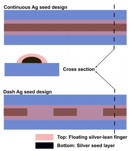
Schematic design of silver-saving metallization structure
TOPCon Solar Cell Low-Silver Metallization Research MethodologyTwo-Step Printing TOPCon Metallization Process
The core of screen-printed silver reduction is a two-step printing TOPCon metallization process: a small amount of conventional silver paste is first printed as a seed layer, creating a high-quality metal-silicon interface. Then, floating finger lines and sink bars are printed using alternating silver-sparing pastes. This screen-printed silver reduction technique ensures excellent metal-silicon interface quality while easing material compatibility requirements, achieving both silver consumption optimization and contact resistance optimization. The photovoltaic metallization process benefits from decoupling interface quality from bulk conductor cost in TOPCon low-silver metallization.
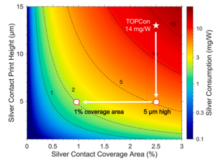
TOPCon Cell Silver Consumption - Contact Coverage as a Function of Print Height
Silver Dot Matrix Seed Layer Contact DesignThe silver dot matrix structure reduces silver contact coverage by printing intermittent dots. This silver dot matrix seed layer contact design enables flexible contact resistance optimization via dot spacing adjustment. The silver dot matrix structure (14 μm width, 50 μm length, 0.43% area) maximizes silver consumption optimization while preserving metal-silicon interface integrity, embodying the floating finger silver reduction design principle in TOPCon low-silver metallization.
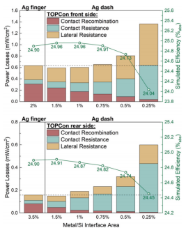
Simulation of cell efficiency and loss decomposition of TOPCon cells with standard silver finger wires and dot matrix structures
Quokka 3 Numerical Simulation Efficiency EvaluationQuokka 3 numerical simulation evaluated the silver dot matrix structure impact on performance, completing Quokka 3 simulation TOPCon efficiency loss analysis. Parameters reflect industrial TOPCon solar cells: wafer size, thickness, body resistivity, minority carrier lifetime, busbar count, finger width/spacing, contact resistivity, passivation interface, emitter sheet resistivity, and polysilicon doping density — all critical photovoltaic metallization process inputs governing solar cell efficiency in TOPCon low-silver metallization.
Experimental Design for TOPCon Low-Silver Metallization
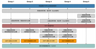
Process flow for preparation of silver-saving metallized TOPCon cells
TOPCon Screen Printing Parameter Configuration and SinteringNon-metallized industrial TOPCon solar cell precursors used n-type Cz wafers (130 μm, 0.6-1.2 Ω·cm). For TOPCon screen printing parameter configuration, five groups were tested: Groups 1-2 printed intermittent silver dots on the rear, conventional silver finger wires/busbars/solder joints on the front, with standard sintering parameters. Groups 3-4 applied silver-coated copper fingers or pure copper on both sides. Group 5 used only high-temperature aluminum paste, with all screen printing parameters completed pre-sintering. Large-area (182×182 mm²) TOPCon solar cells validated the industrial viability of screen-printed silver reduction in TOPCon low-silver metallization.
Experimental procedure: the experiment was divided into five groups:Groups 1 and 2: intermittent silver dots were printed on the rear surface of the TOPCon precursor, followed by conventional silver finger wires, busbars, and solder joints on the front, and an industry-standard sintering process was performed.
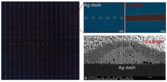
Surface topography characterization after silver-sparing metallization of TOPCon cells
Groups 3 and 4: Silver dots are printed on both the front and back surfaces, followed by the printing of silver clad copper or pure copper finger wires, busbars and solder joints.
Group 5: Only high-temperature pastes were used, omitting the low-temperature curing step, and all screen-printing steps were completed prior to the sintering process.
Sample selection: Preparation of a large area (182 x 182 mm²) TOPCon solar cell using two commercially available burn-through silver pastes for the front and back sides.
Parameter Configuration: The screen parameters and patterning are detailed in the table below, with a silver dot matrix of 14 μm width, 50 μm length and 0.43% area.
Silver Consumption Optimization and Material ComparisonCopper-Based Paste Alternative Efficiency Comparison
In the copper-based paste alternative scheme, TOPCon solar cells with rear-side silver dots achieved 24.95% with silver-coated copper fingers and 25.05% with pure copper — a 0.1-0.2% gap from standard silver. The silver-coated copper finger TOPCon efficiency comparison shows solar cell efficiency loss mainly from 0.5-1% fill factor (FF) decrease due to reduced metal-silicon interface area and higher contact resistance. TOPCon contact resistance optimization methods and screen printing parameters tuning can narrow this gap, validating copper fingers replacing silver fingers TOPCon as a viable copper-based paste alternative for TOPCon low-silver metallization.
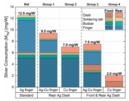
Comparison of Silver Consumption in TOPCon Cells (Multiple Metallization Schemes)
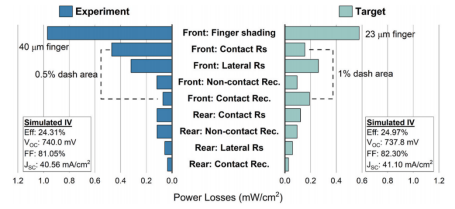
Simulation of efficiency loss and optimization path for double-sided silver-sparing metallization schemes
High-Temperature Aluminum Paste TOPCon Failure AnalysisThe double-sided low-silver screen-printed TOPCon process with Ag dots and Al fingers showed severe degradation: VOC dropped 25 mV, fill factor (FF) fell over 10%, efficiency at only 21.5% (3.5% loss). High-temperature aluminum paste TOPCon failure analysis revealed high-temperature aluminum paste reacting with silver dots during sintering parameters, causing aluminum diffusion that damages the metal-silicon interface. Photoluminescence imaging (PL imaging defect detection) and SEM confirmed the failure mechanism, guiding future photovoltaic metallization process improvements in TOPCon low-silver metallization.
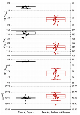
I-V Parameter Degradation of Rear Surface Aluminum Finger Line Scheme
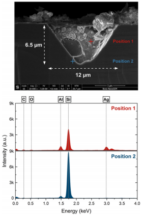
Failure analysis of silver dot/aluminum finger line interface
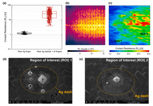
Aluminum-based scheme contact resistance with evidence of material degradation (a) contact resistance comparison (b) photoluminescence PL image (c) contact resistance distribution map (d) and (e) scanning electron microscope image of region 1/2
PL Imaging Defect Detection and Interface CharacterizationPL Imaging Metal-Silicon Interface Defect Analysis
PL imaging defect detection via blue-light excitation captures metallization defects, forming the core of PL imaging metal-silicon interface defect analysis. The PL/EL all-in-one tester photovoltaic cell defect testing system simulates sunlight, uniformly illuminates samples, and captures photoluminescence imaging (PL) and electroluminescence (EL) signals through a professional lens. With 400-1200 nm spectral response, blue-light PL source, and multi-defect identification (pockmarking, darkening, edge intrusion), high-resolution PL imaging defect detection has become the cornerstone diagnostic tool for TOPCon low-silver metallization interface failure analysis, enabling screen-printed silver reduction process optimization.
Frequently Asked Questions
Q1: How is the TOPCon cell 80% silver reduction metallization scheme implemented?
Through screen-printed silver reduction using a silver dot matrix structure and floating finger design, TOPCon low-silver metallization achieves 85% reduction in TOPCon rear-side silver paste and industrial-grade TOPCon silver consumption 7 mg/W total.
Q2: Does industrial-grade TOPCon silver consumption 7 mg/W hurt efficiency?
Solar cell efficiency loss is only 0.1-0.2%, from 0.5-1% fill factor (FF) reduction. Optimizing TOPCon screen printing parameter configuration and sintering parameters enables balanced silver consumption optimization.
Q3: What is the silver dot matrix seed layer contact design principle?
Silver paste is printed as intermittent dot contacts, enabling contact resistance optimization via spacing adjustment. This silver dot matrix seed layer contact design minimizes coverage while preserving metal-silicon interface quality — the foundation of TOPCon contact resistance optimization methods.
Q4: What advantages does PL imaging metal-silicon interface defect analysis offer?
PL imaging defect detection non-destructively identifies metal-silicon interface degradation. The PL/EL all-in-one tester photovoltaic cell defect testing with intelligent software has become essential for TOPCon low-silver metallization R&D.
Q5: How does the silver-coated copper finger TOPCon efficiency comparison measure up?
Silver-coated copper achieves 24.95% vs. pure copper 25.05% — a 0.1% difference. This validates copper fingers replacing silver fingers TOPCon in the copper-based paste alternative pathway, with TOPCon contact resistance optimization methods to close the remaining gap.
Q6: What does high-temperature aluminum paste TOPCon failure analysis reveal?
High-temperature aluminum paste interacts with silver dots during sintering parameters, causing aluminum diffusion into the metal-silicon interface, dropping fill factor (FF) >10% and efficiency by 3.5%. Not recommended for double-sided low-silver screen-printed TOPCon process.
Conclusion
This screen-printed silver reduction technology for TOPCon low-silver metallization uses a silver dot matrix structure and floating finger design on both surfaces, achieving 85% silver consumption optimization down to industrial-grade TOPCon silver consumption 7 mg/W with solar cell efficiency loss of 0.1-0.2%. Further screen printing parameters, sintering parameters, and contact resistance optimization can match standard silver designs. This screen-printed silver reduction pathway enables sustainable TOPCon solar cells manufacturing, advancing photovoltaic metallization process cost reduction through TOPCon low-silver metallization.
Millennial PL/EL All-in-One Tester
E-mail: market@millennialsolar.com
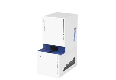
Millennial PL/EL All-in-One Tester simulates sunlight irradiation on a chalcogenide solar cell wafer, uniformly illuminates the whole sample, and captures photoluminescence (PL) signals with a professional lens to obtain PL imaging; electroluminescence (EL) signals to obtain EL imaging. The captured PL/EL imaging is processed and analyzed by image algorithms and software, and PL/EL defects are identified, analyzed, classified, and summarized according to their characteristics.
EL/PL imaging with 5 megapixels for multiple imaging accuracy switching
Spectral response range: 400nm~1200nm
PL light source: blue light (light source size, wavelength, etc. can be customized)
Multiple defects identification analysis (pockmarking, darkening, edge intrusion, etc.) can be customized for defect types
Millennial PL/EL all-in-one tester in this article in photoluminescence (PL) analysis, through the blue light excitation to accurately capture the metallization interface defects. The high-resolution imaging capability and intelligent defect analysis features have become the cornerstone tool for interface failure diagnosis in TOPCon low-silver metallization studies.
Related Products


