
Quantum Efficiency Tester
PL/EL Integrated System
PV-Reflectumeter
3D Confocal Microscope
In-Line Four Point Probe Tester
Four Point Probe Tester
In-Line Thin Film Thickness Tester
Raman Spectrometer
FTIR Spectrometer
Spectrophotometer
Automatic Spectroscopic Ellipsometer
Contact Resistance Tester
Ultra depth of field 3D microscope
Auto Visual Tester
VMM PV Vision Measuring Machine
Solar Cell Horizontal Tensile Tester
Steady State Solar Simulator for Solar Cell
Solar Cell UV Aging Test Chamber
Solar Cell Comprehensive Tensile Tester
Visual Inspection Tester
Wet Leakage Current Tester
PV Module EL Tester
PV Module UV Preconditioning Chamber
Steady State Solar Simulator for PV Module
Current Continuous Monitor
Potential Induced Degradation Test
Bypass Diode Tester
LeTID Test System
Reverse Current Overload Tester
Impulse Voltage Tester
Hipot Insulation Tester
Ground Continuity Tester
Hipot Insulation Ground Tester
Damp Heat Test Chamber
Humidity Freeze Test
Thermal Cycle Test Chamber
Dynamic Mechanical Load Tester
Static Mechanical Load Tester
Hail Impact Tester
Robustness of Termination Tester
Module Breakage Tester
Cut Susceptibility Tester
Peel Shear Strength Tester
Universal Testing Machine (Single-arm)
Universal Testing Machine (Double-arm)
Glass Transmittance Tester
Acetic Acid Test Chamber
EVA Degree of Crosslinking Test System
Junction Box Comprehensive Tester
Drop ball tester
Semi-automatic scanning four-probe tester
Stylus Profilometer
Maximum Power Point Tracker
Perovskite Glass Transmittance Tester
Perovskite P1 Laser Scribing Multifunctional Testing Machine
Perovskite Online PL Tester
Perovskite Online Sheet Resistance Tester
Online Perovskite Film Thickness Tester
Perovskite Process Inspection Workstation
Portable EL Tester
Portable Thermal Imaging Tester
Solar Module Multi-Channel Testing System
PV Inverter Power Quality Tester
Drone EL Tester
IV Tester
IVEL Cell Sorting Machine
Basic Introduction to IBC Solar Cells
Date : 11 January 2024Views : 2290
The solar industry has paved the way for solar panels with higher power using different solar cell technologies that attempt to reduce power losses, increase efficiency and reduce the production cost of photovoltaic (PV) modules. One of the most innovative ways to demonstrate greater efficiency using crystalline silicon (c-Si) cells is interdigitated back contact (IBC) solar cell technology. This issue of Millennial Solar will explain the materials and structure of IBC solar cells and explain how the technology works.
What is IBC solar cell
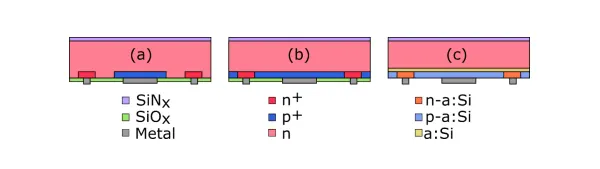
The main component of most IBC solar cells is a c-Si wafer as an n-type wafer absorber layer, but p-type wafers are also used. Monocrystalline silicon (monocrystalline c-Si) is the most common choice due to its higher efficiency, but polycrystalline silicon (polyc-Si) is also available.
An anti-reflective and passivation layer is placed on one of the two sides of the c-Si wafer with a thin layer of silicon dioxide (SiO2) placed through a thermal oxidation process. Materials such as silicon nitride (SiNx) or boron nitride (BNx) are also suitable.
In order for IBC solar cells to relocate the front contacts to the back of the cell, they require interspersed or interdigitated nand emitter layers, called diffusion layers. To create it, layers of an n-type wafer are doped with boron through masked diffusion, masked ion implantation, or laser doping, creating p-type digits while the n-type layer remains intact.
Metal contacts are also placed via laser ablation or wet chemical deposition, using conventional metals such as silver, nickel or copper as contacts for IBC solar cells.
This is one of the most popular methods of making IBC solar cells, there are different methods available but require different materials to make the diffusion layer.
Structure of IBC solar cells
Fabricating IBC solar cells can be quite complex given the formation of diffusion layers, but understanding their structure is relatively simple.
The main layer of an IBC solar cell is an n-type or p-type c-Si wafer that acts as an absorber layer. This layer is made by doping the c-Si layer with boron or phosphorus to create p-type or n-type doped wafers. An anti-reflective and passivating coating, usually made of SiO, is then placed on one or both sides of the solar cell.
The main structural design modification of IBC solar cells is the inclusion of diffusion layers, which feature intersecting n- and p-type layers that allow for the mounting of backside metal contacts.
Finally, each of the IBC solar cells' metal contacts is placed on the back of the cell, leaving the front of the cell completely free of shading material. This also allows the contacts to be installed over a wider area, thus reducing the series resistance of the cell.
How IBC solar cells work
IBC solar cells generate solar energy under the photovoltaic effect, just like Al-BSF solar cells. The load is connected between the positive and negative electrodes of the IBC solar panel, and the photons are converted into electrical energy, generating solar energy to power the load.
Like conventional solar cells, photons strike the IBC solar cell absorber layer, exciting electrons and creating electron-holes (e-h). Because IBC solar panels do not have front metal contacts that shade the cells, these solar cells have a higher conversion area for photons to hit.
The e-h pairs formed on the front side of the IBC solar cell are then collected by the p-type finger layer on the back side. The collected electrons flow from the pmetal contact to the load, generating electricity, and then back to the IBC solar cell through the nmetal contact, ending with specific e-h.
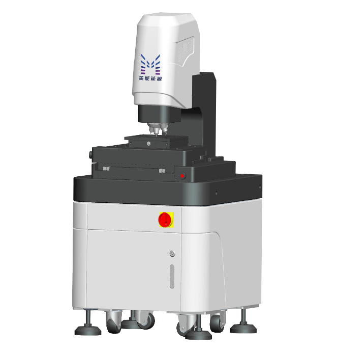
3D Microscope
The 3D Microscope ME-PT3000 is a high-speed confocal scanning microscope for accurate and reliable 3-dimensional (3D) measurements. Real-time confocal microscopy images are achieved through fast optical scanning modules and signal processing algorithms.
ME-PT3000 3D Microscope is an optical instrument specially used in the photovoltaic industry to inspect the quality of grid lines and textures on the surface of photovoltaic cells. Based on the principle of optical technology, combined with precision Z-direction scanning module, 3D modeling algorithm, etc., the device surface is non-contactly scanned and a 3D image of the surface is established. The height and width of the grid lines on the photovoltaic cells and the texture on the surface are measured through the system software. The number of pyramids is quantitatively tested to provide feedback on the quality of photovoltaic cell cleaning, texturing and screen printing processes.
E-mail: market@millennialsolar.com
The basic situation of IBC cell is introduced here first in this issue. Every new solar cell technology is a new possibility for us, and Millennial Solar will always bring you various new sharings.


