
Quantum Efficiency Tester
PL/EL Integrated System
PV-Reflectumeter
3D Confocal Microscope
In-Line Four Point Probe Tester
Four Point Probe Tester
In-Line Thin Film Thickness Tester
Raman Spectrometer
FTIR Spectrometer
Spectrophotometer
Automatic Spectroscopic Ellipsometer
Contact Resistance Tester
Ultra depth of field 3D microscope
Auto Visual Tester
VMM PV Vision Measuring Machine
Solar Cell Horizontal Tensile Tester
Steady State Solar Simulator for Solar Cell
Solar Cell UV Aging Test Chamber
Solar Cell Comprehensive Tensile Tester
Visual Inspection Tester
Wet Leakage Current Tester
PV Module EL Tester
PV Module UV Preconditioning Chamber
Steady State Solar Simulator for PV Module
Current Continuous Monitor
Potential Induced Degradation Test
Bypass Diode Tester
LeTID Test System
Reverse Current Overload Tester
Impulse Voltage Tester
Hipot Insulation Tester
Ground Continuity Tester
Hipot Insulation Ground Tester
Damp Heat Test Chamber
Humidity Freeze Test
Thermal Cycle Test Chamber
Dynamic Mechanical Load Tester
Static Mechanical Load Tester
Hail Impact Tester
Robustness of Termination Tester
Module Breakage Tester
Cut Susceptibility Tester
Peel Shear Strength Tester
Universal Testing Machine (Single-arm)
Universal Testing Machine (Double-arm)
Glass Transmittance Tester
Acetic Acid Test Chamber
EVA Degree of Crosslinking Test System
Junction Box Comprehensive Tester
Drop ball tester
Semi-automatic scanning four-probe tester
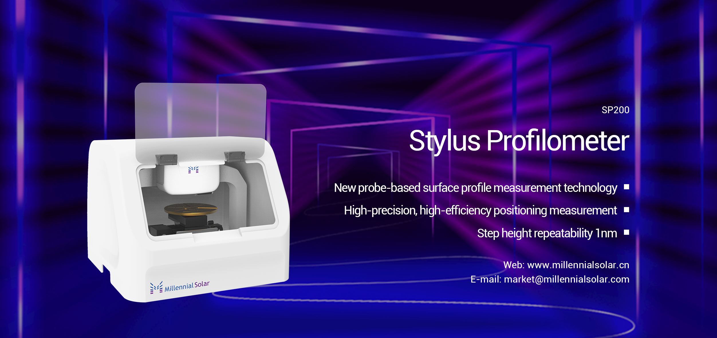
Stylus Profilometer
Maximum Power Point Tracker
Perovskite Glass Transmittance Tester
Perovskite P1 Laser Scribing Multifunctional Testing Machine
Perovskite Online PL Tester
Perovskite Online Sheet Resistance Tester
Online Perovskite Film Thickness Tester
Perovskite Process Inspection Workstation
Portable EL Tester
Portable Thermal Imaging Tester
Solar Module Multi-Channel Testing System
PV Inverter Power Quality Tester
Drone EL Tester
IV Tester
IVEL Cell Sorting Machine
Introduction to Perovskite Solar Cell Production Line Process
Date : 13 March 2024Views : 1730
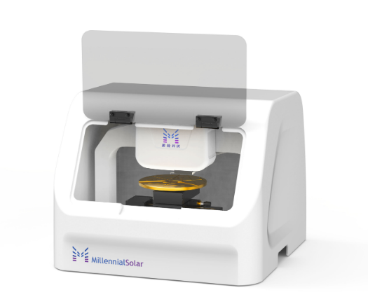
Perovskite solar cells contain perovskite structural compounds as light-harvesting active layers, which have the characteristics of wide absorption spectrum, fast charge separation, long electron and hole transmission distance, and long carrier separation lifetime. But compared with other mature technologies, perovskite solar cell technology is still in the early stages of commercialization. The main issues in the actual device manufacturing of perovskite solar cells are film quality and thickness. Millennial SP200 Stylus Profilometer can help users perfectly control everything from laboratory research and development to production line quality control. It can automatically confirm the accurate thickness of the film on the entire silicon surface through multi-point automatic measurement at different positions, and achieve accurate measurement without contact damage.
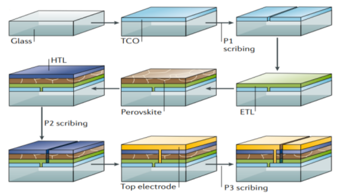
Perovskite solar cell manufacturing process
The perovskite production line process mainly includes coating, printing, etching and packaging. At present, the production technology route of perovskite has not been standardized, and different perovskite solar cell manufacturers often adopt different processes and technology routes.

The fabrication process of a perovskite solar cell
Coating
The coating process to prepare functional layers and electrode layers is a key process for perovskite. The preparation process of the hole transport layer, perovskite layer, electron transport layer, TCO layer and back electrode all involves coating. The coating process of perovskite components mainly uses physical vapor deposition technology (PVD), that is, under vacuum conditions, low-voltage, high-current arc discharge technology is used to evaporate the target material and ionize the evaporated substances and gases using gas discharge. , causing the evaporated substances and their reaction products to be deposited on the workpiece.
According to different reaction methods, the PVD process can be divided into evaporation, magnetron sputtering and reactive plasma plating (RPD), among which:
① The evaporation maturity is high and the film purity is high, but the process temperature is high and the film adhesion is poor. It is mainly used in metal and organic material electrodes;
② The film produced by magnetron sputtering has strong adhesion and low process temperature but may cause uneven thickness. It is mainly used for metal oxide electrodes;
③The film quality of RPD is higher, the bombardment damage to the substrate is smaller, and the film formation speed is faster, but the equipment cost is higher.
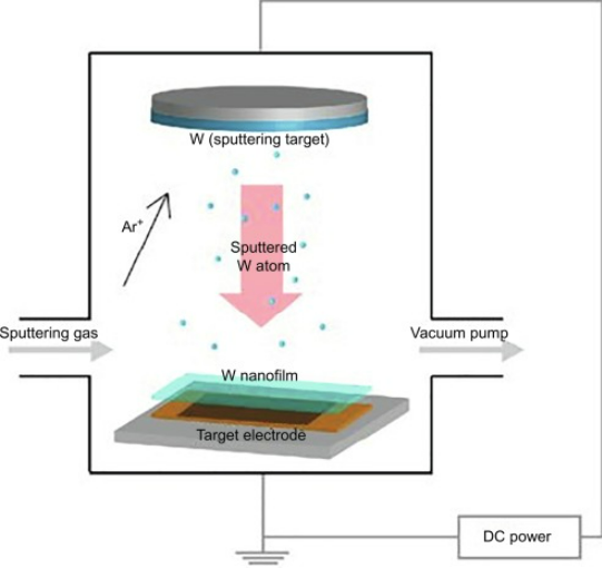
physical vapor deposition technology (PVD)
Coating/printing
Coating and printing processes are mainly used to produce perovskite layers, and attempts to use these two technologies to produce hole and electron transport layers have already begun in the laboratory. Among them, the wet coating process has strong controllability and has become a mainstream process; while the printing process is used to produce printed perovskite components and has a limited scope of application.
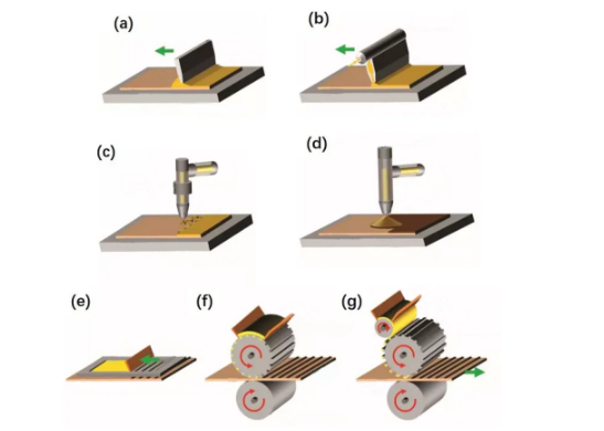
Coating and printing process: (a) Blade coating, (b) Slit coating, (c) Inkjet printing, (d) Spray coating, (e) Screen printing, (f) Letterpress printing (g) Gravure printing
Coating technology can be divided into blade coating, roller coating and slot coating, among which slot coating is the mainstream process.
① Slit coating technology is a high-precision coating method. The working principle is that the coating liquid is squeezed and sprayed along the gap of the coating die and transferred to the substrate. It has the characteristics of fast coating speed, high precision and wet thickness. It has the advantages of uniformity, high slurry utilization rate, and multi-layer coating at the same time.
②The working principle of scraper coating is to use a scraper to scrape off excess paint on the substrate. The specific working principle is to apply excess slurry on the film substrate, and scrape off the excess slurry when the substrate passes between the coating roller and the scraper. This forms a uniform coating on the surface of the substrate, and the gap between the scraper and the substrate determines the thickness of the coating. The advantage is that it is easy to control the coating amount and coating accuracy, and is suitable for slurries with high solid content and high viscosity. However, this kind of scraper may cause damage to the device surface during the scraping process.
③The working principle of roller coating is that the rotation of the coating roller drives the slurry, the amount of slurry transfer is adjusted through the blade gap, and the rotation of the back roller and coating roller is used to transfer the slurry to the substrate. The advantages and disadvantages are similar to those of blade coating.
Etching link
The etching process is used to cut sub-cells, and laser etching has become a mainstream method. The main purpose of laser etching is to use laser scribing to open the film layer and block conduction, thereby forming separate modules and realizing cell slicing. It is mainly used for P1, P2 and P3 layers. Usually, P1 is TCO conductive glass, P2 is perovskite light-absorbing layer, and P3 is usually gold-plated or silver-plated material. In the process of laser etching, it is generally necessary to ensure the accuracy of the laser etching line width and etching line spacing, and not cause damage to the previous layers. The P4 layer mainly uses laser equipment to achieve laser edge cleaning, insulate the edges of the cells, and remove ineffective areas.
Perovskite laser process
Packaging method
In order to avoid damage to the perovskite structure or other functional layers caused by external environmental factors and decomposition leakage, encapsulation is the most effective solution. Common packaging methods can be roughly divided into two categories: one is full coverage packaging, usually preparing a packaging layer on top; the other is edge packaging, where sealant is placed around the module.
For complete coverage of packaging, polymers can be used as packaging materials, or atomic deposition can be used to prepare thin films that isolate water and oxygen. The advantage is that the protection effect is better, but it has a greater impact on the perovskite layer and other functional layers, and due to It is in direct contact with the perovskite functional layer, so it has high requirements on its light transmittance.
The advantage of edge encapsulation is that it can reduce the impact on the contact layer and reduce the possibility of side reactions between the encapsulation material and the perovskite. At the same time, the requirements for the light transmittance of the material are lower, but the encapsulation effect will be reduced accordingly. In order to further increase the water blocking effect, a desiccant can be added during the edge sealing process. Packaging equipment can be shared with the crystalline silicon industry.
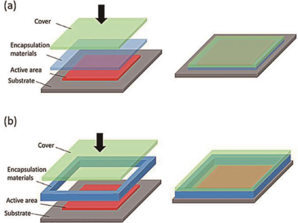
(a) The protective layer is used as a packaging material to cover the active area; (b) The sealant is placed on the edge of the active area
Stylus Profilometer
E-mail: market@millennialsolar.com
The Millennial SP200 Stylus Profilometer uses contact surface topography measurement, which is a breakthrough development in traditional surface topography measurement. The accurate thickness of the film on the entire cell can be confirmed through automatic measurement at multiple points at different locations. The SP200 has excellent measurement repeatability to provide users with accurate film thickness and stress measurements.
● Equipped with 5 million pixel high-resolution color camera
● Sub-angstrom resolution, step height repeatability 1nm
● 360° rotating θ platform combined with Z-axis lifting platform
●Ultra-micro force constant force sensor ensures accurate measurement without contact damage
In order to provide a clear direction for further improving the performance of efficient and stable perovskite solar cells, Millennial Solar proposes perovskite photovoltaic cell research and development solutions and can provide professional perovskite/tandem solar cell process control and testing equipment to help customers design and regulate the components of perovskite materials and other functional layers, develop new film-forming methods, optimize solar cell device structures, and promote perovskite solar cells towards the commercial development of the industry.


