
Quantum Efficiency Tester
PL/EL Integrated System
PV-Reflectumeter
3D Confocal Microscope
In-Line Four Point Probe Tester
Four Point Probe Tester
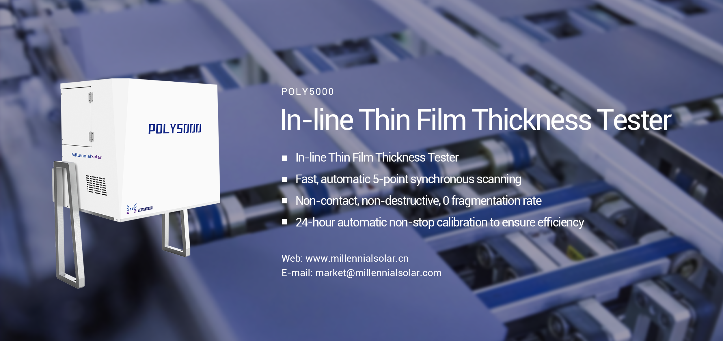
In-Line Thin Film Thickness Tester
Raman Spectrometer
FTIR Spectrometer
Spectrophotometer
Automatic Spectroscopic Ellipsometer
Contact Resistance Tester
Ultra depth of field 3D microscope
Auto Visual Tester
VMM PV Vision Measuring Machine
Solar Cell Horizontal Tensile Tester
Steady State Solar Simulator for Solar Cell
Solar Cell UV Aging Test Chamber
Solar Cell Comprehensive Tensile Tester
Visual Inspection Tester
Wet Leakage Current Tester
PV Module EL Tester
PV Module UV Preconditioning Chamber
Steady State Solar Simulator for PV Module
Current Continuous Monitor
Potential Induced Degradation Test
Bypass Diode Tester
LeTID Test System
Reverse Current Overload Tester
Impulse Voltage Tester
Hipot Insulation Tester
Ground Continuity Tester
Hipot Insulation Ground Tester
Damp Heat Test Chamber
Humidity Freeze Test
Thermal Cycle Test Chamber
Dynamic Mechanical Load Tester
Static Mechanical Load Tester
Hail Impact Tester
Robustness of Termination Tester
Module Breakage Tester
Cut Susceptibility Tester
Peel Shear Strength Tester
Universal Testing Machine (Single-arm)
Universal Testing Machine (Double-arm)
Glass Transmittance Tester
Acetic Acid Test Chamber
EVA Degree of Crosslinking Test System
Junction Box Comprehensive Tester
Drop ball tester
Semi-automatic scanning four-probe tester
Stylus Profilometer
Maximum Power Point Tracker
Perovskite Glass Transmittance Tester
Perovskite P1 Laser Scribing Multifunctional Testing Machine
Perovskite Online PL Tester
Perovskite Online Sheet Resistance Tester
Online Perovskite Film Thickness Tester
Perovskite Process Inspection Workstation
Portable EL Tester
Portable Thermal Imaging Tester
Solar Module Multi-Channel Testing System
PV Inverter Power Quality Tester
Drone EL Tester
IV Tester
IVEL Cell Sorting Machine
Effect of Poly Layer Thickness on the Electrical Performance of N-type TOPCon Cells
Date : 13 August 2024Views : 1440
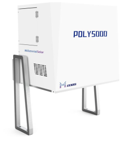
TOPCon solar cells with ultra-thin silicon oxide SiOx film and phosphorus-doped polysilicon Poly layer have a theoretical efficiency limit of up to 28.7%, becoming a hot research technology in the industry. TOPCon cells show superior passivation quality at the metal-silicon contact interface, with higher carrier selectivity and lower recombination rate. However, n+Poly layers of different thicknesses will affect the microstructure formed by the metallized contact, the passivation effect and the electrical performance of the cell. Millennial In-line Thin Film Thickness Tester is designed for photovoltaic process monitoring to help customers accurately obtain film thickness distribution information at different locations of the sample, monitor the stability of the process in real time, and thus optimize the film thickness.
Doped polysilicon is usually crystallized from an amorphous silicon layer a-Si after high temperature heat treatment. Typically, the preparation methods include PECVD, LPCVD, atmospheric pressure CVD, high pressure CVD, sputtering and electron beam evaporation. By studying the parameters of the passivation contact, such as the structural properties and thickness of the SiOx film and the Poly layer and the metallization of the passivation contact, it can provide valuable insights into the influence of the deposition preparation process parameters on the Poly layer and the cell performance.
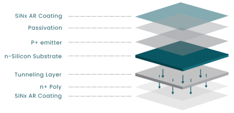
Schematic diagram of TOPCon solar cell structure
By controlling the interface defects of the SiOx film and the doping concentration of the Poly layer, the doped Poly layer can obtain good passivation performance and low contact resistivity. The thickness of the Poly layer can be changed by controlling the deposition process method. Different thicknesses will affect the saturation current density, metallization composite and contact resistivity ρc of the emitter.
Below we measure and analyze polysilicon Poly layers with thicknesses of 30nm, 50nm, 70nm, and 100nm.
Sheet resistance R□
When the thickness of the n+Poly layer decreases from 100nm to 30nm, the sheet resistance (R□) of the cell increases from 45.1 to 57.2Ω/sq. This is because the thickness of the Poly layer determines the total doping amount. Although the surface doping concentration is the same, as the thickness continues to increase, the total doping amount also increases, resulting in a decrease in the sheet resistance of the cell.
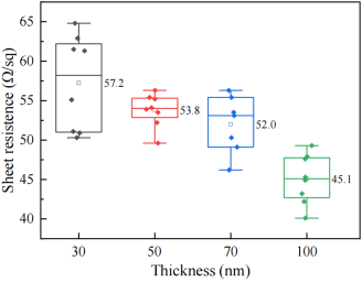
Sheet resistance diagram of TOPCon solar cells with different n+Poly layer thickness
Contact resistivity ρc
When the thickness of the n+Poly layer increases from 30nm to 100nm, the contact resistivity decreases significantly. As the thickness increases, the total doping concentration also increases, thereby narrowing the width of the depletion region inside the silicon wafer and promoting the quantum tunneling effect of carriers through the Schottky barrier. A thicker Poly layer can provide more doping atoms and reduce contact resistivity.

Contact resistivity ρc diagram of TOPCon solar cells with different n+Poly layer thickness
I-V parameters
The thinner n+Poly layer (30 nm) cannot provide sufficient doping concentration and passivation effect, resulting in lower efficiency Eff and open circuit voltage Voc. When the n+Poly layer thickness is 70 nm and 100 nm, the efficiency Eff, open circuit voltage Voc and fill factor FF of the solar cell are all optimal. This shows that these two thicknesses can provide good electrical performance and balanced doping concentration and resistance characteristics.
Table. I-V parameters of TOPCon solar cells with different n+Poly layer thicknesses
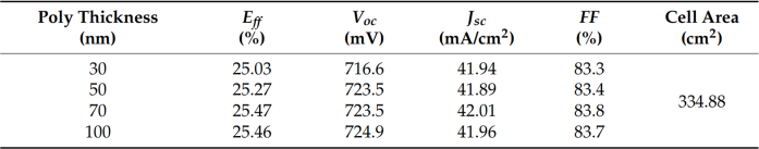

I-V parameters of TOPCon solar cells with different n+Poly layer thicknesses
From the above, it can be concluded that the thickness of the Poly layer has a significant impact on the electrical performance of TOPCon solar cells. Thicker Poly layers have lower sheet resistance and provide higher conductivity. This also shows that when designing and manufacturing solar cells, the thickness of the Poly layer needs to be optimized, which is critical to achieving high-efficiency TOPCon solar cells.
In-line Thin Film Thickness Tester
E-mail: market@millennialsolar.com
In-line Thin Film Thickness Tester can complete the precise detection of thin film thickness while connecting to the industrial detection process, so that battery manufacturers can use this equipment for large-scale systematic detection in the deposition process production line, thereby helping battery manufacturers to greatly save detection time, improve production efficiency and quality assurance!
· Poly film thickness test range 20nm-2000nm
· Fast, automatic 5-point synchronous scanning
· Non-contact, non-destructive measurement, zero fragmentation rate
· 24-hour automatic and non-stop calibration to ensure production efficiency
In practical applications, optimizing the thickness of the Poly layer can achieve a better balance between performance and cost, and achieve the overall efficiency and economy of n-TOPCon solar cells. In-line Thin Film Thickness Tester is designed specifically for photovoltaic process monitoring, helping customers to accurately obtain film thickness distribution information at different locations of the sample, monitor the stability of the process in real time, and thus optimize the film thickness.


