
Quantum Efficiency Tester
PL/EL Integrated System
PV-Reflectumeter
3D Confocal Microscope
In-Line Four Point Probe Tester
Four Point Probe Tester
In-Line Thin Film Thickness Tester
Raman Spectrometer
FTIR Spectrometer
Spectrophotometer
Automatic Spectroscopic Ellipsometer
Contact Resistance Tester
Ultra depth of field 3D microscope
Auto Visual Tester
VMM PV Vision Measuring Machine
Solar Cell Horizontal Tensile Tester
Steady State Solar Simulator for Solar Cell
Solar Cell UV Aging Test Chamber
Solar Cell Comprehensive Tensile Tester
Visual Inspection Tester
Wet Leakage Current Tester
PV Module EL Tester
PV Module UV Preconditioning Chamber
Steady State Solar Simulator for PV Module
Current Continuous Monitor
Potential Induced Degradation Test
Bypass Diode Tester
LeTID Test System
Reverse Current Overload Tester
Impulse Voltage Tester
Hipot Insulation Tester
Ground Continuity Tester
Hipot Insulation Ground Tester
Damp Heat Test Chamber
Humidity Freeze Test
Thermal Cycle Test Chamber
Dynamic Mechanical Load Tester
Static Mechanical Load Tester
Hail Impact Tester
Robustness of Termination Tester
Module Breakage Tester
Cut Susceptibility Tester
Peel Shear Strength Tester
Universal Testing Machine (Single-arm)
Universal Testing Machine (Double-arm)
Glass Transmittance Tester
Acetic Acid Test Chamber
EVA Degree of Crosslinking Test System
Junction Box Comprehensive Tester
Drop ball tester
Semi-automatic scanning four-probe tester
Stylus Profilometer
Maximum Power Point Tracker
Perovskite Glass Transmittance Tester
Perovskite P1 Laser Scribing Multifunctional Testing Machine
Perovskite Online PL Tester
Perovskite Online Sheet Resistance Tester
Online Perovskite Film Thickness Tester
Perovskite Process Inspection Workstation
Portable EL Tester
Portable Thermal Imaging Tester
Solar Module Multi-Channel Testing System
PV Inverter Power Quality Tester
Drone EL Tester
IV Tester
IVEL Cell Sorting Machine
TOPCon Cell Efficiency Improvement: Laser Oxidation Integrates TOPCon Front Surface Poly-Fingers Contacts
Date : 16 July 2025Views : 2180
Although double-sided TOPCon cells (DS-TOPCon) have a high open-circuit voltage (>728 mV), the full-area polysilicon poly-Si layer on the front surface leads to severe light parasitic absorption - >1 mA/cm² of current can be lost at 200 nm thickness. Conventional schemes to thin the poly-Si deteriorate the metallization contact, whereas a selective zone structure (where the poly-Si exists only under the metal gate line) can balance optical and electrical performance.
In this paper, we analyze an innovative process for the preparation of selected zone poly-fingers contacts on the front surface of TOPCon solar cells using nanosecond UV laser oxidation. In optimizing the process, we employed a Millennial 3D confocal microscope for high-precision 3D imaging of the surface morphology and defect analysis to support the development of the constituent structures.
Research Methods
Sample Preparation
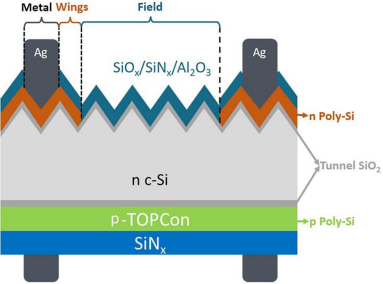
Schematic of a back-junction selective region bifacial TOPCon solar cell
Symmetric structure: n-poly-Si/SiO₂/n-Si/SiO₂/n-poly-Si, substrate 3 Ω-cm n-type CZ wafers (bifacial suede).
Tunneling oxide layer: 15 Å SiO₂ prepared in HNO₃ solution (100°C).
Polysilicon deposition: 200 nm n-type poly-Si grown by LPCVD (588°C).
Laser Patterning Process
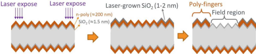
Schematic diagram of laser oxidation mask and polysilicon etching flow
This study proposes a three-stage innovative flow:
Laser oxidation: 355nm nanosecond laser (≥3W, 400mm/s) grows 1-4nm stoichiometric SiO₂ on the TOPCon surface;
Selective etching: KOH solution (9%/40°C) removes 200nm poly-Si in the mask-free region to form 100μm wide poly-Si-fingers;
Passivation Repair: PECVD deposition of 70 nm SiNₓ to compensate for laser damage and compatible with screen-printed metallization.
Results and Discussion
Optical Modeling
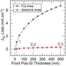
Simulation of photogenerated current loss for full-area vs. selective TOPCon
Effect of polysilicon thickness on current loss:
Full-area TOPCon: Jₛc loss >1 mA-cm-² at thickness >20 nm.
Selective TOPCon (100 μm wide finger zone): Jₛc loss only 0.2 mA-cm-² at 200 nm thick, insensitive to thickness variations (0.3 mA-cm-² loss at 500 nm).
Laser oxidation mechanism
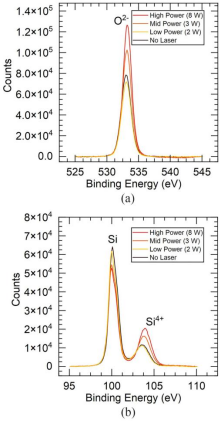
XPS profiles of (a) O²- peak and (b) Si⁴⁺ peak at different laser powers
Oxide layer characterization: XPS confirms the generation of dense SiO₂ with O²- enrichment (532 eV) and Si⁴⁺ peak offset (103.5 nm) at laser power ≥ 3 W, which is consistent with the Deal-Grove thermal oxidation model;
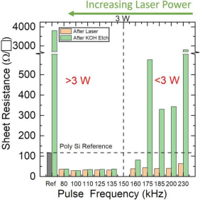
Measurements of cube resistance of poly-Si films before and after KOH etching
Etching selectivity: after 3W laser, the poly-Si square resistance stays ~30 Ω/□, indicating that the SiO₂ mask resists KOH etching for 90 seconds; below 3W, the mask fails.
Damage repair and passivation recovery
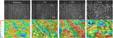
Laser confocal microscopy images (top view vs. isometric view)
Laser damage: power >3W leads to pyramidal weave rounding and J₀ spike ≤2300 fA/cm²;
Hydrogen passivation repair: after 70 nm PECVD SiNₓ deposition, J₀ at 3W laser drops to 43.2 fA/cm² (of which the laser surface contributes 36.8 fA/ cm²), and the selected poly-Si-fingers area composite is only 1.65 fA/cm² (4.48% coverage).
Cell simulation (Quokka 2)
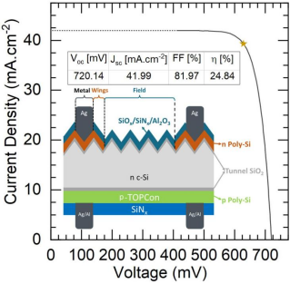
Simulated current-voltage characteristic curves of selective front surface bifacial TOPCon solar cells
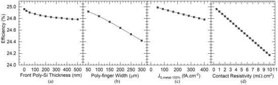
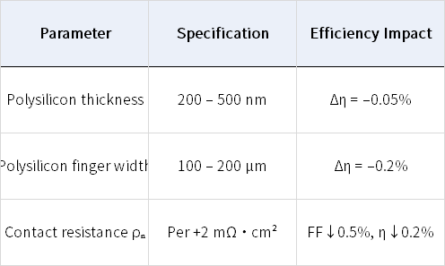
Simulated solar cell efficiency as a function of (a) polysilicon finger thickness, (b) finger width, (c) metal contact J0, (d) contact resistivity
Baseline efficiency: 24.84% (J₀,metal=300 fA-cm-², contact resistivity 2 mΩ-cm²).
Sensitivity analysis of key parameters:
Thickness of polysilicon (200→500 nm): efficiency reduced by 0.05%.
Finger width (100→200 μm): efficiency reduced by 0.2% (Vₒc↓2.1 mV, Jₛc↓0.4 mA-cm-².
Metal contact J₀ (300→50 fA-cm-²): efficiency increased to 25%.
Contact resistance (per 2 mΩ-cm-² increase): ↓0.5% FF and ↓0.2% efficiency.
Industrialization path validated by Quokka2 cell simulation:
Process compatibility:
Fully compatible with screen printing production line (including 760°C sintering)
Eliminates 5 processes of traditional photolithography/TMAH etching, cost reduction ≥18%
Efficiency boundary:
Efficiency up to 25.0% (initial value 24.84%) at J0,metal ≤ 50 fA/cm²
In this paper, we analyze an innovative process for the preparation of front surface-selected polycrystalline silicon (poly-Si) contacts for TOPCon solar cells using nanosecond UV laser oxidation. The process realizes retaining only the poly-Si contact strip below the metal grid line by laser-induced growth of SiO₂ mask combined with KOH selective etching, which effectively solves the problem of light parasitic absorption of the full-area poly-Si layer on the front surface in conventional bifacial TOPCon cells. Experiments show that this solution significantly improves optical transmittance while maintaining excellent passivation performance, providing a new path for 25%+ efficient batteries.
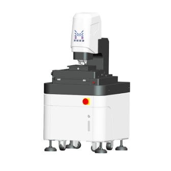
Millennial 3D Confocal Microscope
email:market@millennialsolar.com
Millennial 3D confocal microscope ME-PT3000 is an optical instrument specialized in the photovoltaic industry for quality inspection of grid lines and velvet on the surface of photovoltaic substrates. The depth and width of the grid lines on the PV substrate and the number of pyramids on the velvet surface are quantitatively inspected to provide feedback on the process quality of the PV substrate.
Accurate and reliable 3D measurement for real-time confocal microscopy images
Ultra-high confocal lens with Z-axis display resolution up to 1nm
High precision and repeatability
Fully automated raster velvet measurement for fast data generation
Millennial 3D confocal microscopes are used throughout the process for sub-micron inspection of surface gratings and velvet, ensuring controlled optimization of optical performance.
Related Products


