
Quantum Efficiency Tester
PL/EL Integrated System
PV-Reflectumeter
3D Confocal Microscope
In-Line Four Point Probe Tester
Four Point Probe Tester
In-Line Thin Film Thickness Tester
Raman Spectrometer
FTIR Spectrometer
Spectrophotometer
Automatic Spectroscopic Ellipsometer
Contact Resistance Tester
Ultra depth of field 3D microscope
Auto Visual Tester
VMM PV Vision Measuring Machine
Solar Cell Horizontal Tensile Tester
Steady State Solar Simulator for Solar Cell
Solar Cell UV Aging Test Chamber
Solar Cell Comprehensive Tensile Tester
Visual Inspection Tester
Wet Leakage Current Tester
PV Module EL Tester
PV Module UV Preconditioning Chamber
Steady State Solar Simulator for PV Module
Current Continuous Monitor
Potential Induced Degradation Test
Bypass Diode Tester
LeTID Test System
Reverse Current Overload Tester
Impulse Voltage Tester
Hipot Insulation Tester
Ground Continuity Tester
Hipot Insulation Ground Tester
Damp Heat Test Chamber
Humidity Freeze Test
Thermal Cycle Test Chamber
Dynamic Mechanical Load Tester
Static Mechanical Load Tester
Hail Impact Tester
Robustness of Termination Tester
Module Breakage Tester
Cut Susceptibility Tester
Peel Shear Strength Tester
Universal Testing Machine (Single-arm)
Universal Testing Machine (Double-arm)
Glass Transmittance Tester
Acetic Acid Test Chamber
EVA Degree of Crosslinking Test System
Junction Box Comprehensive Tester
Drop ball tester
Semi-automatic scanning four-probe tester
Stylus Profilometer
Maximum Power Point Tracker
Perovskite Glass Transmittance Tester
Perovskite P1 Laser Scribing Multifunctional Testing Machine
Perovskite Online PL Tester
Perovskite Online Sheet Resistance Tester
Online Perovskite Film Thickness Tester
Perovskite Process Inspection Workstation
Portable EL Tester
Portable Thermal Imaging Tester
Solar Module Multi-Channel Testing System
PV Inverter Power Quality Tester
Drone EL Tester
IV Tester
IVEL Cell Sorting Machine
Photovoltaic Module Anomalies: Analysis of Causes for Corner Defects and Fragmentation at Cell Solder Ribbon Locations
Date : 1 September 2025Views : 8390
During photovoltaic module production, various anomalies inevitably occur, leading to module downgrading. Among these, corner defects (chipped corners) and microcracks at cell solder ribbon locations are two common anomalies with complex and diverse causes. The following section provides a detailed analysis of key scenarios contributing to these anomalies.
As a specialized equipment manufacturer focused on the long-term reliability and performance of photovoltaic modules, Millennial Solar module testing equipment strictly adheres to the internationally recognized IEC 61215 standard. Its testing capabilities deeply align with the quality control requirements for various ground-mounted crystalline silicon photovoltaic modules, helping to prevent process anomalies such as solder ribbon side standing at their source.
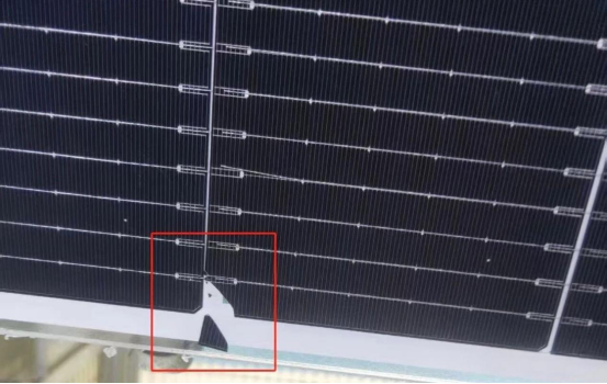
I. Standing Up of Flattened Welding Ribbons
During the string welding process, the circular welding ribbons between two solar cells are flattened by a dedicated flattening mechanism. This aims to increase the contact area between the ribbon and the cell edges, reduce localized pressure in this region, and prevent mechanical damage to the cells.
However, if the flattening mechanism malfunctions during production (e.g., uneven pressure, component misalignment) or the ribbon traction mechanism operates abnormally (e.g., speed fluctuations, positioning errors), the flattened ribbon may “stand upright.” This drastically reduces contact area with the cell, causing localized pressure to surge and ultimately leading to microcracks or corner chipping in the cell.
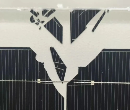
II. Excessively Narrow Cell Spacing or “V-Shaped Gap”
In TOPCon module production, when connecting two cells in series via the busbar, the busbar must connect the rear surface of the preceding cell to the front surface of the following cell. Therefore, precise control of cell spacing is critical—even after flattening, the busbar thickness remains between 0.1-0.15mm. If the cell spacing is too narrow, the compressive force on the interconnect at the junction between two cells increases significantly, making it highly susceptible to hidden cracks or chipped corners.
Additionally, the “eight-character gap” is another typical contributing factor: this refers to the spacing between two solar cells exhibiting an “eight-shaped” configuration where one side is wider than the other. On the narrower side, the stronger compression from the solder ribbon similarly leads to frequent microcracks or chipped corners.
It is important to note: If chipping at the solder ribbon location is accompanied by “small fragments (adjacent to the solder ribbon),” this anomaly is primarily caused by direct solder ribbon compression on the cell. It is strongly correlated with factors such as excessively narrow cell spacing, solder ribbon thickness exceeding specifications after flattening (excessively thick), and deviations in the flattening and stretching position.
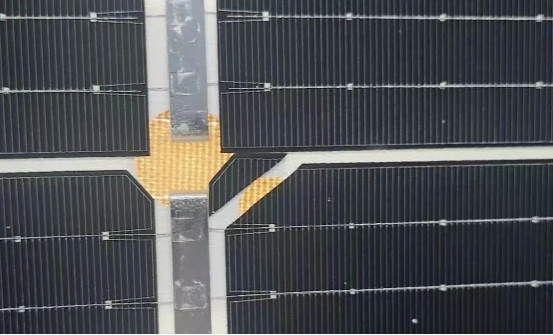
III. Abnormalities During Double-Glass Encapsulation
During the encapsulation process of double-glass modules, operational anomalies—such as uneven encapsulation pressure, adhesive film placement deviations, or module positioning shifts—can also cause microcracks or corner chipping at the solder ribbon location.
The typical characteristic of such corner chipping is that, since the stress occurs before the lamination process, the chipped fragments are usually separated from the cell body by a considerable distance. As shown in the figure above: the chipped fragments are mostly small, scattered pieces that have completely detached from the cell body and been carried to the module edge by the flowing adhesive film during the edge sealing process.
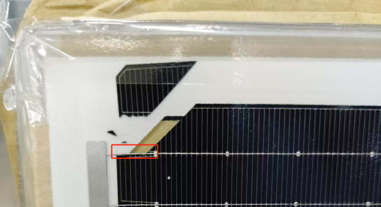
IV. High Temperature Causing Glass Warping and Deformation
If no obvious abnormalities are observed in the center hole area of the module after lamination, but chipping occurs at the solder tab positions along the cell edges, and after ruling out the three factors mentioned above, the lamination temperature control should be prioritized for investigation: If the module experiences a sudden temperature rise (rather than a gradual increase) after entering the laminator, the glass may warp due to uneven heating. This warping induces additional stress at the cell solder tab positions, ultimately causing chipping at the center hole location.
Such chipped fragments also exhibit significant spacing from the main cell body. This can be improved through the following two methods:
1. Reduce the set temperature of the laminator chamber and slow the heating rate;
2. Replace the lower high-temperature cloth with one of 0.79mm thickness. By adjusting the thermal conductivity of the high-temperature cloth, the heating rate of the glass is indirectly slowed.
V. Residual Tin Balls and Tin Residue on the Solder Ribbon Surface
During the string welding process, inadequate solder paste melting (e.g., insufficient melting temperature, too short melting time, abnormal flux usage) may cause isolated solder balls to form on the solder ribbon surface or leave partially melted solder residue. Such contaminants adhere tightly to the ribbon surface. When subsequently entering the first chamber of the laminator for lamination:
Negative pressure generated during vacuum extraction;
Positive pressure exerted by the silicone pad on the glass during lamination;
Two types of pressure indirectly transmit to solder balls/residue on the solder ribbon surface, causing localized pressure concentration at the contact point between the cell and solder ribbon. This ultimately leads to cell corner chipping or breakage.
From early warning signs of solder ribbon standing up, to quantitative control of cell spacing deviations, to identifying pressure concentration risks caused by solder balls and debris, various anomalies in PV module production that lead to solder ribbon corner chipping and microcracks fundamentally require a “precision detection + process linkage” solution. As a specialized equipment service provider focused on the long-term reliability and performance of photovoltaic modules, Millennial Solar supporting inspection equipment strictly adheres to the IEC 61215 international standard, deeply aligning with the quality control requirements for various ground-mounted crystalline silicon photovoltaic modules.
Related Solutions

IEC61215 & IEC61730 Testing Standards
Millennial Solar: Precision testing equipment meeting global IEC standards.
View DetailsRelated Products


