
Quantum Efficiency Tester
PL/EL Integrated System
PV-Reflectumeter
3D Confocal Microscope
In-Line Four Point Probe Tester
Four Point Probe Tester
In-Line Thin Film Thickness Tester
Raman Spectrometer
FTIR Spectrometer
Spectrophotometer
Automatic Spectroscopic Ellipsometer
Contact Resistance Tester
Ultra depth of field 3D microscope
Auto Visual Tester
VMM PV Vision Measuring Machine
Solar Cell Horizontal Tensile Tester
Steady State Solar Simulator for Solar Cell
Solar Cell UV Aging Test Chamber
Solar Cell Comprehensive Tensile Tester
Visual Inspection Tester
Wet Leakage Current Tester
PV Module EL Tester
PV Module UV Preconditioning Chamber
Steady State Solar Simulator for PV Module
Current Continuous Monitor
Potential Induced Degradation Test
Bypass Diode Tester
LeTID Test System
Reverse Current Overload Tester
Impulse Voltage Tester
Hipot Insulation Tester
Ground Continuity Tester
Hipot Insulation Ground Tester
Damp Heat Test Chamber
Humidity Freeze Test
Thermal Cycle Test Chamber
Dynamic Mechanical Load Tester
Static Mechanical Load Tester
Hail Impact Tester
Robustness of Termination Tester
Module Breakage Tester
Cut Susceptibility Tester
Peel Shear Strength Tester
Universal Testing Machine (Single-arm)
Universal Testing Machine (Double-arm)
Glass Transmittance Tester
Acetic Acid Test Chamber
EVA Degree of Crosslinking Test System
Junction Box Comprehensive Tester
Drop ball tester
Semi-automatic scanning four-probe tester
Stylus Profilometer
Maximum Power Point Tracker
Perovskite Glass Transmittance Tester
Perovskite P1 Laser Scribing Multifunctional Testing Machine
Perovskite Online PL Tester
Perovskite Online Sheet Resistance Tester
Online Perovskite Film Thickness Tester
Perovskite Process Inspection Workstation
Portable EL Tester
Portable Thermal Imaging Tester
Solar Module Multi-Channel Testing System
PV Inverter Power Quality Tester
Drone EL Tester
IV Tester
IVEL Cell Sorting Machine
Bypass Diodes in Solar Panels
Date : 7 November 2025Views : 1670
Various issues may arise during the operation of Solar Panels in power plants, leading to a loss of power generation. One such issue is the breakdown of bypass diodes in junction boxes. Below is a brief introduction to bypass diodes in Solar Panels.
I. Bypass Diodes for Solar Panels
The commonly used bypass diodes in Solar Panels are electronically termed Schottky diodes. Named after their inventor, Dr. Schottky, SBD stands for Schottky Barrier Diode. Unlike PN junction diodes formed by contacting P-type and N-type semiconductors, SBDs are fabricated using the metal-semiconductor junction principle, where a metal (e.g., gold, silver, platinum) contacts a semiconductor.
II. Structure of the Schottky Diode
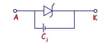
Equivalent Circuit of a Schottky Diode
A Schottky diode is formed by connecting a doped semiconductor region (typically N-type) to a metal (such as gold, silver, or platinum). It features a metal-semiconductor junction rather than a PN junction, as illustrated below.
Equivalent Circuit of a Schottky Diode
Because a Schottky diode involves metal-semiconductor contact, it lacks the charge storage mechanism present in PN diodes. When switching the electric field, there is no delay caused by the need to first dissipate stored charge. Consequently, Schottky diodes exhibit extremely fast switching response times. This is one of the key reasons they are selected as bypass diodes. When hot spots occur in solar cells, high currents can be instantly bypassed, providing the fastest protection. Once the hot spot disappears, the bypass diode immediately returns to its cutoff state, allowing the module to resume maximum power output. Thus, the ultra-high switching response frequency of Schottky diodes precisely meets the application requirements of solar modules.
III. Operating Principle of Bypass Diodes
Bypass diodes are typically connected in parallel with two series strings of solar cells. When a cell or a string becomes shaded, the shaded cells cease to generate electricity and instead act as resistive loads. As the resistance increases to a certain threshold, the corresponding bypass diode activates. This bypasses the shaded string, The module current then flows through the bypass diode, preventing excessive heat generation caused by current flowing through the shaded cells and ensuring the module's normal operation.
IV. Failure of Bypass Diodes
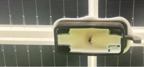
Failure of the bypass diode
Common failure modes for bypass diodes include inability to withstand high temperatures and high current surges. When partial shading triggers the bypass diode to conduct, the high forward current causes rapid heating. Under other adverse conditions—such as loose solder joints in the junction box or prolonged operation of the diode—breakdown is likely to occur.
① Poor Soldering: Weak connections exist at the junction between the diode leads and copper conductors within the junction box, as well as between the busbar and copper conductors. When shading or other issues activate the bypass diode, these solder joints overheat. If the accumulated heat exceeds the thermal deformation temperature of the junction box insulation material, the box will age and deform. The longer the bypass diodes remain activated, the greater the risk of junction box deformation and aging. When temperatures exceed the upper limit of the diode junction temperature, the high heat can cause thermal breakdown and damage to the bypass diodes, potentially even burning out the junction box.
② Hot Spots: Under prolonged conditions such as shading, microcracks, or localized hot spots, the bypass diode remains in continuous operation. This causes the junction temperature to rise. Once the accumulated junction temperature reaches a critical level, the bypass diode undergoes thermal breakdown and fails. If not addressed promptly, heat accumulation may reach the deformation temperature of the junction box insulation material, causing deformation and aging. In severe cases, this can lead to junction box burnout.
③ Lightning Strikes: When a PV module is struck by lightning, improper or non-compliant grounding can cause the bypass diode to instantly break down under high voltage. After the storm clears, as normal module current flows through the failed diode over time, the diode generates heat. Once heat accumulates to a certain level, it can cause the junction box to age and deform, or even burn out. (Lightning strikes typically leave impact marks on the module frame)
V. Testing Standards for Bypass Diodes
① GB/T 44081—2024/IEC 62979:2017 “Thermal Runaway Testing for Bypass Diodes in Solar Panels”
② IEC 61215-2:2021 “Functional Testing and Thermal Performance Testing of Bypass Diodes”


