
Quantum Efficiency Tester
PL/EL Integrated System
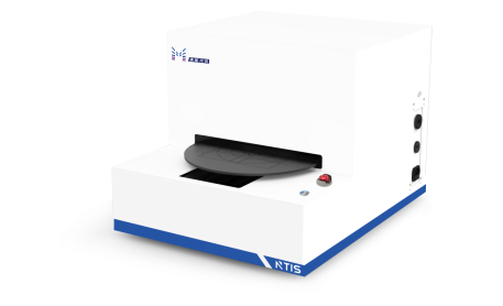
PV-Reflectumeter
3D Confocal Microscope
In-Line Four Point Probe Tester
Four Point Probe Tester
In-Line Thin Film Thickness Tester
Raman Spectrometer
FTIR Spectrometer
Spectrophotometer
Automatic Spectroscopic Ellipsometer
Contact Resistance Tester
Ultra depth of field 3D microscope
Auto Visual Tester
VMM PV Vision Measuring Machine
Solar Cell Horizontal Tensile Tester
Steady State Solar Simulator for Solar Cell
Solar Cell UV Aging Test Chamber
Solar Cell Comprehensive Tensile Tester
Visual Inspection Tester
Wet Leakage Current Tester
PV Module EL Tester
PV Module UV Preconditioning Chamber
Steady State Solar Simulator for PV Module
Current Continuous Monitor
Potential Induced Degradation Test
Bypass Diode Tester
LeTID Test System
Reverse Current Overload Tester
Impulse Voltage Tester
Hipot Insulation Tester
Ground Continuity Tester
Hipot Insulation Ground Tester
Damp Heat Test Chamber
Humidity Freeze Test
Thermal Cycle Test Chamber
Dynamic Mechanical Load Tester
Static Mechanical Load Tester
Hail Impact Tester
Robustness of Termination Tester
Module Breakage Tester
Cut Susceptibility Tester
Peel Shear Strength Tester
Universal Testing Machine (Single-arm)
Universal Testing Machine (Double-arm)
Glass Transmittance Tester
Acetic Acid Test Chamber
EVA Degree of Crosslinking Test System
Junction Box Comprehensive Tester
Drop ball tester
Semi-automatic scanning four-probe tester
Stylus Profilometer
Maximum Power Point Tracker
Perovskite Glass Transmittance Tester
Perovskite P1 Laser Scribing Multifunctional Testing Machine
Perovskite Online PL Tester
Perovskite Online Sheet Resistance Tester
Online Perovskite Film Thickness Tester
Perovskite Process Inspection Workstation
Portable EL Tester
Portable Thermal Imaging Tester
Solar Module Multi-Channel Testing System
PV Inverter Power Quality Tester
Drone EL Tester
IV Tester
IVEL Cell Sorting Machine
n-type Back-Contact BC Cell: Optimizing Antireflection and Surface Passivation Properties via SiNx/SiON Layered Structure
Date : 14 November 2025Views : 1355
Back-contact back-junction (BC BJ) cells significantly enhance carrier collection efficiency by integrating the emitter and metal contacts onto the rear surface. This study employs a non-vacuum interruption method to fabricate a SiNx/SiON bilayer structure. Combining Quokka and Essential Macleod simulations, it systematically optimizes the structure's antireflection and passivation properties. This approach integrates the passivation advantages of silicon-rich SiNx with the antireflection characteristics of SiON while simplifying the fabrication process. Experimental data from a Millennial velvet reflectometer confirms the anti-reflection advantage of the SiNx/SiON stack over a true velvet structure, providing critical in-situ validation for optical simulation results.
Preparation of SiNx/SiON Stack
Passivation performance testing utilized commercial n-type Czochralski silicon wafers (Cz-Si) (thickness 200 μm, resistivity 0.3–2 Ω·cm); Optical and electrical characterization utilized n-type single-sided polished wafers (resistivity 1–10 Ω·cm). Samples underwent NaOH/NaOCl treatment to remove dicing damage, RCA1 solution to eliminate organic impurities, followed by diluted HF etching to remove the native SiO₂ oxide layer.
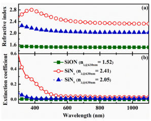
Refractive index (a) and extinction coefficient (b) of silicon-rich SiNx layer, SiON top layer, and single-layer SiNx in SiNx/SiON stacked structures
Continuous deposition of dual-layer films via PECVD non-vacuum interruption method avoids contamination from vacuum exposure, enhancing process stability and reducing costs.
Silicon-rich SiNₓ layer:
Gas ratio: SiH₄:NH₃:Ar = 1.25:1:12.5 (100:80:1000 sccm);
Process conditions: Substrate temperature 400°C, RF power 300 W (13.56 MHz), chamber pressure 1 Torr, target refractive index n≈2.41.
SiON Layer:
Gas ratio: SiH₄:NH₃:N₂O:Ar = 1:2.66:2.66:12.5 (100:266:266:1250 sccm);
Process conditions: Substrate temperature 300°C, other parameters identical to SiNₓ layer, target refractive index n≈1.52.
Optical Properties of SiNx/SiON Layers
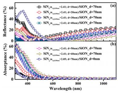
Essential Macleod simulation-based curves of (a) reflectance and (b) absorptance: Performance comparison of SiNx/SiON layers with varying silicon-rich SiNx thicknesses versus single-layer SiNx on crystalline silicon (c-Si)
The combination of SiNₓ (high refractive index) and SiON (low refractive index) achieves broadband antireflection. Simulations show that when the silicon-rich SiNₓ thickness increases from 10 nm to 40 nm, the average reflectance in the 300–1100 nm range decreases from 20.23% to 3.45%. However, reflectance increases again when the thickness exceeds 40 nm.
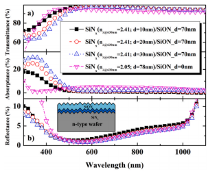
Experimentally measured (a) transmittance versus absorption and (b) reflectance curves: Performance comparison of SiNx/SiON stacked layers with varying silicon-rich SiNx thicknesses and single-layer SiNx on glass and random-textured crystalline silicon (c-Si) substrates
Experimental verification shows that the average reflectance of the 30 nm SiNₓ/70 nm SiON stacked layer is as low as 3.95%, significantly lower than that of the single-layer SiNₓ (6.81%), with a more pronounced reduction in reflectance in the short-wavelength range of 300–500 nm (3.94% vs. 13.39%). Simultaneously, the absorption rate of this stacked layer at this thickness reached 6.89%, higher than that of a single-layer SiNₓ (4.03%), facilitating photogenerated carrier generation.
Passivation Performance of SiNx/SiON Layers
To optimize surface passivation quality, n-type Czochralski single-crystal silicon (Cz n-type c-Si) was used for double-sided deposition of silicon-rich SiNx layers (refractive index n=2.41) at varying thicknesses, followed by a 70 nm SiON layer (n=1.52). Passivation performance was evaluated via effective carrier lifetime (τeff). For all samples, the maximum τeff occurred at a minority carrier density Δn≈2.86×10¹⁴ cm⁻³.
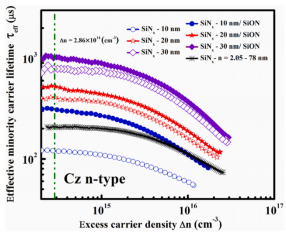
The relationship between carrier effective lifetime and excess carrier concentration (Δn): Comparison of passivation performance on undiffused n-type crystalline silicon (c-Si) samples for deposited SiNx, SiNx capped with SiON (various thicknesses), and monolayer SiNx (n=2.05, thickness=78 nm)
τeff continuously increases as the silicon-rich SiNx thickness rises from 10 nm to 30 nm. This phenomenon is closely related to the mechanism of hydrogen content in SiNx: hydrogen terminates dangling bonds at the interface by forming Si-H bonds, and the Si-H bond density increases synchronously with SiNx thickness (10→30 nm). Electrical characterization further confirms that the 30 nm thick SiNx layer corresponds to the highest fixed charge density (Qf) and lowest density of interface states (Dit).
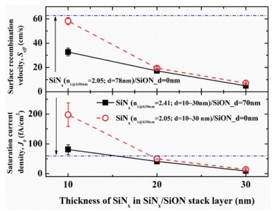
Surface recombination rate (Seff) and saturation current density (J₀) versus SiNx thickness (n=2.41): Comparison of passivation performance between SiNx film, SiNx/SiON multilayer, and single-layer SiNx (n=2.05) on Czochralski (Cz) n-type crystalline silicon wafers
Comparison of passivation effects between SiNx/SiON multilayers of varying thicknesses and single-layer SiNx. Results indicate:
Both surface recombination rate (Seff) and saturation current density (J₀) decrease with increasing SiNx thickness (10→30 nm), reaching minimum values at 30 nm;
All SiNx/SiON stacked layers exhibited significantly lower Seff and J₀ values than the single-layer SiNx (n=2.05, d=78 nm), specifically:
Stacked samples: Seff=4.9 cm/s, J₀=9 fA/cm²
Single-layer sample: Seff = 62.6 cm/s, J₀ = 58 fA/cm²
The performance improvement is attributed to thicker silicon-rich SiNx layers promoting hydrogen atom diffusion toward the c-Si interface, thereby enhancing passivation and reducing carrier recombination. The increase in τeff directly leads to decreases in Seff and J₀. The maximum thickness of SiNx (including SiNx/SiON stacks) is limited to 30 nm.
Quokka Simulation
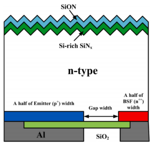
Structural Model of BC BJ Battery Cell in Quokka Simulation
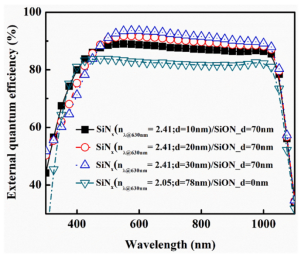
External Quantum Efficiency (EQE) of BC BJ Solar Cells: Performance Comparison of SiNx/SiON Layers with Different Silicon-Rich SiNx Thicknesses versus Single-Layer SiNx (n=2.05, Thickness=78 nm) Across the 300-1100 nm Wavelength Range
External quantum efficiency (EQE) analysis indicates:
In the short-wavelength band of 300–500 nm, the SiNx/SiON stacked cell (containing 10/20/30 nm SiNx) exhibits significantly enhanced EQE, directly attributable to increased light absorption resulting from the thicker silicon-rich SiNx layer;
In the 500–1000 nm band, the stacked cell exhibits a high EQE plateau, with performance ranking as 30 nm > 20 nm > 10 nm. This is attributed to: minimal reflectance variation in this band (specular reflectance: 3.38% for 10 nm, 2.82% for 20 nm, 2.46% for 30 nm); The 30 nm SiNx layer provides optimal passivation;
Front-side passivation quality is critical for charge collection, as carriers in BC BJ cells are primarily generated near the front surface and collected at the rear surface.
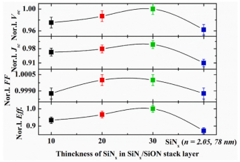
Normalized Performance Parameters (Voc, Jsc, FF, Eff) of BC BJ Cells: Comparison of Devices with Different SiNx/SiON Layered Structures vs. Single-Layer SiNx Coatings
Cell performance comparisons confirm:
Cells with SiNx/SiON layered structures on the front side exhibit higher efficiencies than single-layer SiNx (n=2.05, d=78 nm);
30 nm SiNx-layered cells achieved the highest Jsc and Voc;
Performance advantages stem from the layered structure's high transmittance, low reflectance, and superior passivation effects, collectively enhancing cell Jsc, Voc, and ultimate conversion efficiency.
Results indicate: The synergistic interaction between silicon-rich SiNx (refractive index 2.41) and SiON (refractive index 1.52) reduces the average reflectance of the multilayer to 3.95% across the 300-1100 nm wavelength range, with surface recombination velocity (Seff) as low as 5 cm/s. Compared to single-layer SiNx, the multilayer structure increased the short-circuit current density (Jsc) of the BC BJ cell by 3.4 mA/cm² and the open-circuit voltage (Voc) by 26 mV, ultimately achieving a 14.59% efficiency gain. This process offers a new pathway for low-cost industrialization.
Millennial Diffuse Reflectance Tester
email:market@millennialsolar.com
The Millennial Diffuse Reflectance Tester RTIS excites solar cells via diffuse reflection and then detects them using a spectrometer at an 8-degree angle. RTIS features a positioning platform and guide rails, enabling convenient and rapid sample loading, achieving precise positioning of solar cell samples, and enhancing operator efficiency.
• Spectral measurement range: 350-1050nm
• Rapid, automated multi-point measurement
• Approx. 0.1s per point, reducing testing time to 1/10th of conventional reflectometers
• Precise measurement of critical parameters including reflectance and film thickness
The Millennial Velvet Reflectometer employs 8° diffuse excitation combined with multi-point matrix scanning to achieve in-situ statistical measurement of SiNx/SiON multilayer reflectance on industrial-grade velvet silicon wafers. Its rapid, non-destructive testing capabilities accelerate the transition of this technology from laboratory to production line implementation.
Related Products


