
Quantum Efficiency Tester
PL/EL Integrated System
PV-Reflectumeter
3D Confocal Microscope
In-Line Four Point Probe Tester
Four Point Probe Tester
In-Line Thin Film Thickness Tester
Raman Spectrometer
FTIR Spectrometer
Spectrophotometer
Automatic Spectroscopic Ellipsometer
Contact Resistance Tester
Ultra depth of field 3D microscope
Auto Visual Tester
VMM PV Vision Measuring Machine
Solar Cell Horizontal Tensile Tester
Steady State Solar Simulator for Solar Cell
Solar Cell UV Aging Test Chamber
Solar Cell Comprehensive Tensile Tester
Visual Inspection Tester
Wet Leakage Current Tester
PV Module EL Tester
PV Module UV Preconditioning Chamber
Steady State Solar Simulator for PV Module
Current Continuous Monitor
Potential Induced Degradation Test
Bypass Diode Tester
LeTID Test System
Reverse Current Overload Tester
Impulse Voltage Tester
Hipot Insulation Tester
Ground Continuity Tester
Hipot Insulation Ground Tester
Damp Heat Test Chamber
Humidity Freeze Test
Thermal Cycle Test Chamber
Dynamic Mechanical Load Tester
Static Mechanical Load Tester
Hail Impact Tester
Robustness of Termination Tester
Module Breakage Tester
Cut Susceptibility Tester
Peel Shear Strength Tester
Universal Testing Machine (Single-arm)
Universal Testing Machine (Double-arm)
Glass Transmittance Tester
Acetic Acid Test Chamber
EVA Degree of Crosslinking Test System
Junction Box Comprehensive Tester
Drop ball tester
Semi-automatic scanning four-probe tester
Stylus Profilometer
Maximum Power Point Tracker
Perovskite Glass Transmittance Tester
Perovskite P1 Laser Scribing Multifunctional Testing Machine
Perovskite Online PL Tester
Perovskite Online Sheet Resistance Tester
Online Perovskite Film Thickness Tester
Perovskite Process Inspection Workstation
Portable EL Tester
Portable Thermal Imaging Tester
Solar Module Multi-Channel Testing System
PV Inverter Power Quality Tester
Drone EL Tester
IV Tester
IVEL Cell Sorting Machine
Back-contact IBC solar cells achieve 25.2% efficiency through enhanced passivation and anti-reflective coating technologies
Date : 28 November 2025Views : 1410
IBC solar cells leverage their back-contact design (where all electrodes are positioned on the rear surface) to eliminate light-blocking losses caused by front-side metal busbars, thereby enhancing light absorption efficiency. However, their manufacturing process is complex and costly, with the primary technical challenge lying in achieving effective surface passivation and fine-tuning related parameters. This study systematically analyzed the influence of key parameters—including crystalline silicon (c-Si) bulk lifetime, wafer resistivity, back-side boron-doped layer sheet resistance, and recombination current density (J₀)—on cell performance using Quokka3 simulation software. The Millennial four-probe resistance tester enables rapid, automated scanning of cell samples to obtain sheet resistance/resistivity distribution data across different locations.
Research Methodology
This study simulates the IBC cell structure using Quokka3 software. The simulated cell employs an n-type crystalline silicon (c-Si) wafer as the substrate. The cell front is coated with a passivation layer and anti-reflective coating (ARC) to optimize photon capture and minimize losses. The rear surface features a p⁺-type emitter and an n⁺-type backsurface field (BSF), arranged in an interleaved pattern without physical isolation zones to enhance electrical continuity. Optimized rear passivation/anti-reflective coating and electrode design further reduce recombination losses.
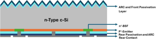
Schematic Diagram of IBC Solar Cell Structure
Key simulation parameters include:
Cell thickness: 150 μm
Wafer resistivity: 0.6–1.8 Ω·cm
Volume lifetime (SRH electron/hole lifetime): 1–5 ms
Emitter sheet resistance: 100–500 Ω/sq
BSF sheet resistance: 35 Ω/sq
Front surface passivation recombination current density J₀: 1–60 fA/cm²
Back surface passivation recombination current density J₀: 1–60 fA/cm²
Emitter/BSF contact resistance: 2×10⁻⁵ Ω·cm²
Effect of c-Si Bulk Lifetime and Wafer Resistivity
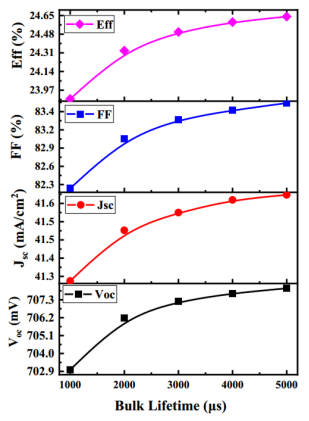
Simulation results of electrical parameters in IBC solar cells as a function of n-type c-Si wafer bulk lifetime
Extending the c-Si bulk lifetime (1–5 ms) significantly enhances Voc, Jsc, FF, and η. Increased bulk lifetime directly reduces carrier recombination rate, thereby decreasing the saturation current density I₀ and leading to higher Voc. Simultaneously, increased carrier diffusion length enhances the collection efficiency of photo-generated carriers, thereby improving Jsc and FF. Simulation results indicate that when the body lifetime reaches 5 ms, the cell efficiency η can reach a maximum of 24.64%, fully demonstrating the critical role of high-quality silicon material in cell performance and reliability.
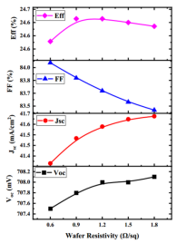
Simulation Results of IBC Solar Cell Electrical Parameters as a Function of n-Type c-Si Wafer Resistivity
The impact of wafer resistivity variation (0.6–1.8 Ω·cm) on cell performance exhibits nonlinear characteristics. Within the 0.6–1.2 Ω·cm range, both Voc and Jsc increase with rising resistivity. This primarily stems from higher resistivity broadening the pn-junction depletion layer width, which reduces bulk recombination losses and enhances absorption of longer-wavelength photons. When resistivity exceeds 1.2 Ω·cm, increased series resistance causes FF to decrease, and efficiency begins to decline after reaching its peak. Simulation results indicate that cell efficiency peaks at 24.65% when resistivity is 1.2 Ω·cm, demonstrating that optimizing wafer resistivity is crucial for balancing material conductivity and recombination losses.
Impact of Back-Side Boron-Doped Layer Sheet Resistance
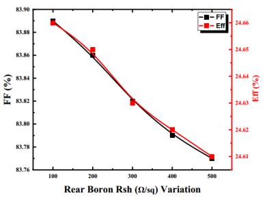
Quokka3 Simulation Results on the Effect of Back Boron Doped Layer Sheet Resistance (Rsh) on FF and η of IBC Solar Cells
Simulation results indicate that an increase in the square resistance Rₛₕ of the rear boron-doped layer leads to a slight decrease in FF and a reduction in conversion efficiency η. This is primarily due to the elevated Rₛₕ increasing the cell's series resistance, hindering efficient carrier collection and transport, and resulting in a deterioration of the I-V curve's “squareness.” Notably, the open-circuit voltage Voc and short-circuit current density Jsc remain largely unaffected by Rₛₕ variations, as they are determined by the material's bandgap and light absorption capacity, respectively. This highlights the significant influence of the back-emitter characteristics on FF, underscoring the critical importance of optimizing boron doping concentration to balance conductivity and recombination.
Effect of recombination current density J₀ on passivation efficiency
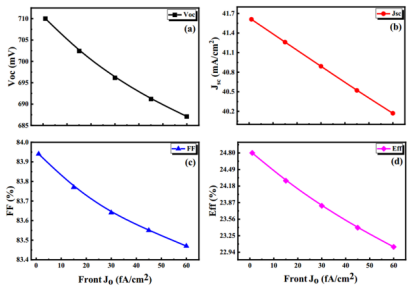
Effect of Front Surface Recombination Layer Composite Current Density (J₀) on Electrical Parameters of Quokka3-Simulated IBC Cells
An increase in front-surface recombination current density J₀ leads to a comprehensive decrease in Voc, Jsc, FF, and η. Higher J₀ values indicate intensified front-surface recombination, reducing the number of photogenerated carriers available for collection and degrading the I-V curve characteristics. Simulation data indicates that efficiency begins to decline significantly when J₀ exceeds approximately 30 fA/cm², underscoring the necessity of applying a high-quality passivation layer on the front surface.
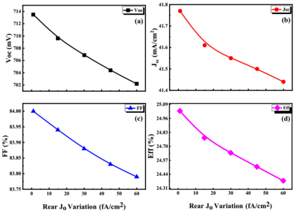
Effect of Back Surface Passivation Layer Recombination Current Density (J₀) on Electrical Parameters of Quokka3-Simulated IBC Cells
Increasing the back recombination current density J₀ similarly reduces Voc, Jsc, FF, and η. For IBC cells, where all charge collection occurs via the back contact, the impact of J₀ on passivation quality is particularly critical. An elevated J₀ directly increases recombination losses in the pn junction bend region, significantly degrading Voc and FF. Selective passivation techniques (e.g., Al₂O₃ on the p⁺ emitter and SiO₂ on the n⁺ BSF) can effectively reduce recombination and enhance Voc. However, the design and passivation of the pn junction region remain sensitive factors affecting the pseudo-fill factor (pFF).
Interaction Between Emitter Coverage and Back Boron Sheet Resistance
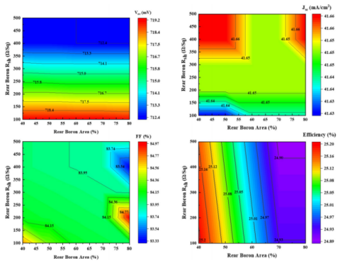
Simulation of the Combined Effect of Back Boron Sheet Resistance and Coverage on IBC Cell Parameters
The synergistic optimization of emitter coverage and back boron sheet resistance is central to achieving peak efficiency. Simulation results indicate that optimal cell performance is achieved at an emitter coverage of approximately 40% and a rear boron block resistance Rₛₕ = 100 Ω/sq: Voc = 719.2 mV, Jsc = 41.66 mA/cm², FF = 84.71%, conversion efficiency η = 25.2%. This optimized point effectively balances recombination losses in the contact area and resistive losses. When coverage falls below 40%, current aggregation effects cause significant loss increases; when coverage exceeds 40%, recombination losses from the large passivated surface area begin to dominate, offsetting the benefits of low contact resistance.
This paper systematically investigates the optimization of passivation and antireflection techniques for IBC solar cells. Through Quokka3 simulations, it reveals the efficiency enhancement mechanisms achieved by fine-tuning c-Si bulk lifetime, sheet resistance, and J₀. For the first time, it integrates the interactive effects of bulk lifetime, resistivity, backside boron sheet resistance, and emitter coverage, achieving a peak efficiency of 25.2% and establishing a new industry benchmark.
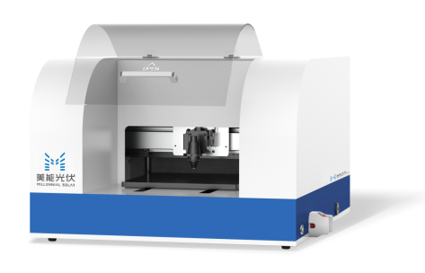
Millennial Four-Probe Resistivity Tester
email:market@millennialsolar.com
The Millennial Four-Probe Resistance Tester enables rapid, automated scanning of samples up to 230mm in size, capturing sheet resistance/resistivity distribution data across different positions. It finds extensive applications in photovoltaics, semiconductors, alloys, ceramics, and numerous other fields.
Ultra-wide measurement range: 1mΩ to 100MΩ
High-precision measurement with dynamic repeatability up to 0.2%
Fully automated multi-point scanning with multiple preset schemes and customizable adjustments
Rapid material characterization with automatic calibration factor calculation
The Millennial Four-Probe Resistance Tester serves as the core experimental equipment for obtaining key electrical parameters of IBC cells. Its role spans the entire process from material screening and process monitoring to performance verification, supporting experimental reproducibility at the 25.2% efficiency optimization point. Its data directly determines the reliability of research conclusions and industrial implementation value.
Related Products


