
Quantum Efficiency Tester
PL/EL Integrated System
PV-Reflectumeter
3D Confocal Microscope
In-Line Four Point Probe Tester
Four Point Probe Tester
In-Line Thin Film Thickness Tester
Raman Spectrometer
FTIR Spectrometer
Spectrophotometer
Automatic Spectroscopic Ellipsometer
Contact Resistance Tester
Ultra depth of field 3D microscope
Auto Visual Tester
VMM PV Vision Measuring Machine
Solar Cell Horizontal Tensile Tester
Steady State Solar Simulator for Solar Cell
Solar Cell UV Aging Test Chamber
Solar Cell Comprehensive Tensile Tester
Visual Inspection Tester
Wet Leakage Current Tester
PV Module EL Tester
PV Module UV Preconditioning Chamber
Steady State Solar Simulator for PV Module
Current Continuous Monitor
Potential Induced Degradation Test
Bypass Diode Tester
LeTID Test System
Reverse Current Overload Tester
Impulse Voltage Tester
Hipot Insulation Tester
Ground Continuity Tester
Hipot Insulation Ground Tester
Damp Heat Test Chamber
Humidity Freeze Test
Thermal Cycle Test Chamber
Dynamic Mechanical Load Tester
Static Mechanical Load Tester
Hail Impact Tester
Robustness of Termination Tester
Module Breakage Tester
Cut Susceptibility Tester
Peel Shear Strength Tester
Universal Testing Machine (Single-arm)
Universal Testing Machine (Double-arm)
Glass Transmittance Tester
Acetic Acid Test Chamber
EVA Degree of Crosslinking Test System
Junction Box Comprehensive Tester
Drop ball tester
Semi-automatic scanning four-probe tester
Stylus Profilometer
Maximum Power Point Tracker
Perovskite Glass Transmittance Tester
Perovskite P1 Laser Scribing Multifunctional Testing Machine
Perovskite Online PL Tester
Perovskite Online Sheet Resistance Tester
Online Perovskite Film Thickness Tester
Perovskite Process Inspection Workstation
Portable EL Tester
Portable Thermal Imaging Tester
Solar Module Multi-Channel Testing System
PV Inverter Power Quality Tester
Drone EL Tester
IV Tester
IVEL Cell Sorting Machine
HJT Cell PVD Process
Date : 19 December 2025Views : 1650
Physical Vapor Deposition (PVD) is a critical step in the fabrication process of HJT heterojunction cells. This technology utilizes a vacuum environment to induce physical evaporation or sputtering of material sources, causing gaseous atoms or molecules to deposit onto the substrate surface and form high-quality thin films. In HJT cell manufacturing, the PVD process is primarily used to prepare the transparent conductive oxide (TCO) layer. This layer significantly impacts the cell's electrical conductivity and optical properties. Excellent electrical conductivity helps reduce series resistance and enhance carrier collection efficiency. Meanwhile, ideal optical properties improve light absorption and minimize reflection losses, playing a decisive role in the cell's overall conversion efficiency.
I. Role and Positioning of PVD in HJT Cells
The structure of an HJT cell, from top to bottom, typically consists of: metal grid lines → transparent conductive oxide (TCO) film → amorphous silicon film (intrinsic layer and doped layer) → crystalline silicon substrate → amorphous silicon film → TCO film → metal grid lines.
The core task of the PVD process here is to deposit a high-quality transparent conductive oxide (TCO) film onto the amorphous silicon films at both ends.
This TCO film serves three critical functions:
1. Lateral Conductivity: Collects photo-generated carriers from the amorphous silicon layers and conducts them to the metal grid lines. Amorphous silicon itself has extremely low lateral conductivity and cannot efficiently collect charge, making the TCO layer an indispensable “conductive highway.”
2. Anti-reflection and transmittance enhancement: Acts as an anti-reflective layer, reducing reflection losses of incident light and increasing the cell's absorption of sunlight.
3. Protective layer: Shields the fragile intrinsic and amorphous silicon layers from damage during subsequent screen printing processes.
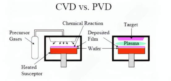
II. Fundamental Principles of PVD Processes
Physical Vapor Deposition (PVD)
PVD is a process that vaporizes solid target materials (raw materials) through physical methods, transports them in a vacuum environment, and ultimately condenses them into solid-state films on substrate surfaces.
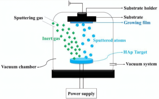
In TCO deposition for HJT cells, magnetron sputtering is the most prevalent PVD technique. Its operating principle can be broken down into the following steps:
1. Establishing the Vacuum Environment: Silicon wafers are loaded into the vacuum chamber and evacuated to a high vacuum level (e.g., 10⁻³ Pa). This eliminates interference from air molecules, prevents target oxidation and film contamination, and ensures film purity and quality.
2. Process gas introduction: High-purity process gas, typically argon, is introduced into the chamber with precisely controlled flow rates. Argon, being an inert gas, does not chemically react with the target material during subsequent discharge processes, hence the term “reactive sputtering.”
3. Plasma generation: A high voltage (usually DC or RF power). Free electrons are accelerated by the electric field. Upon gaining sufficient energy, they collide with argon atoms, ionizing them into argon ions and additional electrons. This avalanche-like process forms a glow plasma within the chamber, composed of numerous electrons and ions.
4. Sputtering Process: Positively charged argon ions are accelerated by the electric field and bombard the surface of the target material connected to the cathode at high speed. This high-energy impact acts like a “billiard ball collision,” transferring momentum to “sputter” atoms or molecules from the target material. These particles are ejected from the target surface and disperse into the surrounding space in gaseous form.
5. Thin Film Deposition: Atomized atoms/molecules from the target material travel through the vacuum chamber, ultimately reaching and depositing onto the silicon wafer surface. These particles migrate, nucleate, and grow on the wafer surface, eventually forming a dense, uniform TCO film.
6.Magnetic Field Enhancement: Specially designed permanent magnets or electromagnets are placed behind the target material to generate a magnetic field. The magnetic field confines electrons, causing them to spiral near the target surface. This significantly increases the collision paths and probability between electrons and argon atoms. Consequently, a high-density plasma can be maintained at lower gas pressures and voltages, substantially boosting sputtering rates while reducing bombardment damage to the silicon wafer from high-energy particles.
III. Technical Key Points and Challenges of HJT-Specific PVD
1. Low-Temperature Process
The amorphous silicon film in HJT cells is extremely temperature-sensitive, typically requiring the entire process chain to remain below 200°C. Therefore, the PVD process must strictly control thermal loading to prevent plasma overheating, which can degrade the amorphous silicon layer's performance (hydrogen outgassing, structural changes).
2. Balancing Film Properties
TCO films require an optimal balance between conductivity and transparency.
Conductivity is determined by carrier concentration and mobility. Carrier concentration is typically enhanced through doping (e.g., Sn in ITO, Zn in IZO) and introducing trace hydrogen during deposition to increase oxygen vacancies.
Transparency demands high transmittance across the visible and near-infrared spectrum. Excessively high carrier concentration induces free carrier absorption in the infrared region, leading to parasitic absorption losses.
Process optimization objective: Identify the optimal process window that maximizes the product of “conductivity × transmittance.”
3. Step Coverage and Damage Control
The surface of HJT cells features a textured structure with micrometer-scale pyramids. PVD requires excellent step coverage on these pyramids to ensure continuous, uniform TCO film coverage across the entire textured surface; otherwise, conductive dead zones will form.
High-energy particles (including reflected argon atoms, secondary electrons, etc.) bombarding the silicon wafer surface may cause “sputtering damage” to the underlying amorphous silicon interface, increasing interface state density and affecting open-circuit voltage. Damage mitigation requires adjusting process parameters such as working pressure, power, and bias voltage.
4. Common TCO Targets
ITO: Indium Tin Oxide, the longest-established material with balanced performance, but indium is expensive and toxic.
IWO/IWO:H: Indium tungsten oxide, featuring higher mobility and lower free carrier absorption at equivalent conductivity. Particularly suited for HJT cells, enabling higher short-circuit current.
IZO: Indium zinc oxide, also an important indium-free or low-indium alternative.
IV. Brief Comparison of PVD and RPD
In the HJT field, another crucial technique for depositing TCO is Reactive Plasma Deposition (RPD). RPD generates TCO films by reacting an oxygen plasma with organometallic sources, enabling superior film properties at lower temperatures—particularly advantageous in minimizing interface damage.
Principle Differences: RPD utilizes arc discharge to evaporate target materials into plasma. This plasma is then guided and filtered by electromagnetic fields to deposit low-energy, high-ionization-rate plasma onto the substrate.
Advantages: Films deposited by RPD exhibit minimal damage and typically higher carrier mobility, enhancing performance.
Disadvantages: High equipment cost, low target material utilization, significant maintenance expenses, and patent barriers.
Current Status: PVD remains the dominant technology in HJT production lines due to its maturity, cost advantages, and balanced performance; RPD finds application in scenarios pursuing extreme efficiency.
The PVD process for HJT cells fundamentally utilizes magnetron sputtering—a physical vapor deposition technique—to deposit TCO films with high electrical conductivity and high light transmittance onto sensitive amorphous silicon layers under low-temperature, vacuum conditions. This process perfectly balances the three critical functions of “conductivity,” “light transmission,” and “protection,” serving as the vital bridge connecting photogenerated carriers within the cell to the external circuit. The level of process mastery directly determines the ultimate efficiency and cost of HJT cells.


