
Quantum Efficiency Tester
PL/EL Integrated System
PV-Reflectumeter
3D Confocal Microscope
In-Line Four Point Probe Tester
Four Point Probe Tester
In-Line Thin Film Thickness Tester
Raman Spectrometer
FTIR Spectrometer
Spectrophotometer
Automatic Spectroscopic Ellipsometer
Contact Resistance Tester
Ultra depth of field 3D microscope
Auto Visual Tester
VMM PV Vision Measuring Machine
Solar Cell Horizontal Tensile Tester
Steady State Solar Simulator for Solar Cell
Solar Cell UV Aging Test Chamber
Solar Cell Comprehensive Tensile Tester
Visual Inspection Tester
Wet Leakage Current Tester
PV Module EL Tester
PV Module UV Preconditioning Chamber
Steady State Solar Simulator for PV Module
Current Continuous Monitor
Potential Induced Degradation Test
Bypass Diode Tester
LeTID Test System
Reverse Current Overload Tester
Impulse Voltage Tester
Hipot Insulation Tester
Ground Continuity Tester
Hipot Insulation Ground Tester
Damp Heat Test Chamber
Humidity Freeze Test
Thermal Cycle Test Chamber
Dynamic Mechanical Load Tester
Static Mechanical Load Tester
Hail Impact Tester
Robustness of Termination Tester
Module Breakage Tester
Cut Susceptibility Tester
Peel Shear Strength Tester
Universal Testing Machine (Single-arm)
Universal Testing Machine (Double-arm)
Glass Transmittance Tester
Acetic Acid Test Chamber
EVA Degree of Crosslinking Test System
Junction Box Comprehensive Tester
Drop ball tester
Semi-automatic scanning four-probe tester
Stylus Profilometer
Maximum Power Point Tracker
Perovskite Glass Transmittance Tester
Perovskite P1 Laser Scribing Multifunctional Testing Machine
Perovskite Online PL Tester
Perovskite Online Sheet Resistance Tester
Online Perovskite Film Thickness Tester
Perovskite Process Inspection Workstation
Portable EL Tester
Portable Thermal Imaging Tester
Solar Module Multi-Channel Testing System
PV Inverter Power Quality Tester
Drone EL Tester
IV Tester
IVEL Cell Sorting Machine
Passivation Mechanism of Al₂O₃ Films
Date : 26 December 2025Views : 1055
The passivation of aluminum oxide films can be categorized into chemical passivation and field-effect passivation. Chemical passivation involves forming a dense oxide layer on the film surface, effectively suppressing non-radiative recombination of charge carriers and enhancing chemical stability at the interface. Field-effect passivation regulates the interface band structure using fixed charges, thereby inhibiting the accumulation of minority carriers on the surface. The combined action of these two mechanisms significantly reduces surface recombination rates, improving the cell's open-circuit voltage and conversion efficiency.
The passivation mechanism of aluminum oxide films in solar cells manifests primarily through two aspects: chemical passivation and field-effect passivation. This dual passivation mechanism is the key reason why aluminum oxide (Al₂O₃) thin films, particularly in crystalline silicon solar cells, achieve exceptional surface passivation performance.
I. Chemical Passivation
Chemical passivation
1. Core Function
To effectively reduce the number of exposed dangling bonds on silicon wafer surfaces, various surface treatment technologies can be employed. Specific methods include hydrogen passivation, oxidation passivation, or chemical modification. These processes form stable chemical bonds, saturating the active sites on the silicon surface and significantly lowering the density of dangling bonds on the material's surface. Such surface modifications not only enhance the material's electrical properties but also improve device interface characteristics, playing a crucial role in semiconductor device manufacturing and performance optimization.
2. Principle
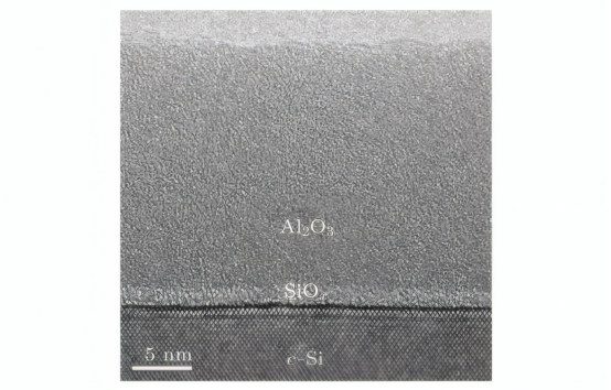
TEM image of a 20nm-thick Al₂O₃ film on monocrystalline silicon
Silicon crystal surfaces contain numerous exposed, unsaturated chemical bonds (dangling bonds). These dangling bonds introduce interface states within the silicon bandgap that facilitate carrier recombination. When a high-quality Al₂O₃ film is deposited onto the silicon surface (typically achieved via atomic layer deposition), aluminum and oxygen atoms in the film react with the silicon surface's dangling bonds, forming stable Si-O-Al or Si-Al bonds. These chemical bonds effectively “saturate” the dangling bonds on the silicon surface, significantly reducing the density of interface states. This, in turn, minimizes non-radiative recombination (Shockley-Read-Hall recombination) of charge carriers at the surface.
3. Effect
Advanced surface repair technologies can effectively eliminate both microscopic defects and macroscopic damage on material surfaces. Surface imperfections such as scratches, pits, and microcracks fall within the scope of repair. This direct repair method significantly optimizes the physicochemical properties of material surfaces, substantially reducing the rate of interfacial recombination processes. Specifically, the repaired surface forms a more uniform and dense protective layer, decreasing the number of active sites and effectively suppressing electron-hole recombination at the interface. Simple to implement and highly effective, this approach provides a practical solution for enhancing material interface performance and overall stability.
II. Field-Effect Passivation
1. Core Mechanism
In the near-surface region of semiconductor silicon materials, an artificially controllable electric field is induced by applying an external bias or constructing a space charge region. This directional electric field exerts a pronounced repulsive or attractive effect on minority carriers (e.g., holes in n-type silicon or electrons in p-type silicon). Through this charge regulation mechanism, minority carriers are effectively driven away from surface regions with high recombination activity, significantly reducing surface recombination rates. This electric field modulation technique enables precise control over carrier spatial distribution, providing an effective means to optimize device surface passivation.
2. Principle
Al₂O₃ films harbor substantial fixed negative charges, typically originating from charge centers within the film—such as defects associated with oxygen vacancies or aluminum vacancies—and inherent material properties.
This fixed charge density is exceptionally high, typically ranging from 10¹² to 10¹³ cm⁻² (far exceeding the positive charge density of SiO₂).
When Al₂O₃ is deposited on p-type silicon (the most common application scenario, e.g., the rear side of PERC cells): the fixed charges induce a positively charged hole accumulation layer (i.e., the accumulation layer) near the p-type silicon surface. Simultaneously, the electric field generated by these charges repels minority carriers (electrons), pushing them away from the silicon/Al₂O₃ interface.
When Al₂O₃ is deposited on n-type silicon: the fixed negative charge induces a negatively charged electron accumulation layer (i.e., the accumulation layer) near the n-type silicon surface. Simultaneously, the electric field generated by this charge attracts minority carriers (holes) toward the interface (an undesirable effect). Consequently, the passivation effect of Al₂O₃ on n-type silicon is typically less effective than on p-type silicon.
3. Effect
For p-type silicon, driving minority carriers (electrons) away from surfaces with high recombination rates significantly reduces electron concentration at the surface, thereby markedly lowering surface recombination rates.
For n-type silicon, attracting minority carriers (holes) to the surface may increase recombination (resulting in poor performance or requiring special treatment).
III. Synergistic Effects of Chemical Passivation and Field-Effect Passivation
On p-type silicon substrate materials (particularly applicable to the typical process scenario of PERC solar cell rear passivation), the outstanding passivation performance of Al₂O₃ films primarily manifests as a dual synergistic effect between chemical passivation mechanisms and field-effect passivation mechanisms. At the microscopic level, the chemical passivation process primarily relies on the stable Si-O covalent bond structure spontaneously formed at the Al₂O₃ film/silicon substrate interface. This structure effectively neutralizes and eliminates recombination centers such as dangling bonds at the interface (significantly reducing the density of interface states). Concurrently, the field-effect passivation mechanism leverages the inherent fixed negative charge properties of the Al₂O₃ film to induce the formation of an accumulation layer on the silicon surface. This layer significantly suppresses the diffusion flux of minority carriers (electrons in this case) toward the surface region.
These two physical mechanisms do not operate independently but produce synergistic enhancement through charge compensation and band structure regulation. Chemical passivation improves interface quality, creating favorable conditions for field-effect passivation; conversely, field-effect passivation further alleviates interface recombination pressure by reducing carrier concentration gradients. It is precisely this complementary interaction that enables the Al₂O₃ passivation layer on p-type silicon surfaces to simultaneously achieve a surface recombination rate below 10 cm/s and an effective carrier lifetime exceeding 1 ms. These performance metrics play a decisive role in enhancing the photovoltaic conversion efficiency of solar cells.
IV. Characterization of Al₂O₃ Passivation Effect
Low Surface Recombination Rate: Direct indicator of superior passivation performance.
High Effective Minority Carrier Lifetime: Determined through quasi-steady-state photocathode measurements or microwave photocathode decay techniques.
High open-circuit voltage: In final solar cell devices, superior rear passivation significantly enhances cell open-circuit voltage.
High built-in potential/field effect: Capacitance-voltage testing reveals elevated fixed negative charge density at the Al₂O₃/Si interface.
The passivation mechanism of alumina films in solar cells manifests as the perfect synergy between chemical passivation and field-effect passivation. Chemical passivation refers to reducing recombination centers by saturating dangling bonds on the silicon surface and lowering the density of interface states. Field-effect passivation involves repelling minority carrier electrons away from the surface of p-type silicon through the repulsive force exerted by high-density fixed negative charges. This dual mechanism makes Al₂O₃ an ideal passivation material for achieving ultra-low surface recombination rates on p-type silicon surfaces. It has played a transformative role, particularly in the back-side passivation of PERC cells, significantly enhancing cell efficiency. Its exceptional passivation performance depends on high-quality film deposition (especially atomic layer deposition (ALD) technology) and appropriate post-processing techniques.


