
Quantum Efficiency Tester
PL/EL Integrated System
PV-Reflectumeter
3D Confocal Microscope
In-Line Four Point Probe Tester
Four Point Probe Tester
In-Line Thin Film Thickness Tester
Raman Spectrometer
FTIR Spectrometer
Spectrophotometer
Automatic Spectroscopic Ellipsometer
Contact Resistance Tester
Ultra depth of field 3D microscope
Auto Visual Tester
VMM PV Vision Measuring Machine
Solar Cell Horizontal Tensile Tester
Steady State Solar Simulator for Solar Cell
Solar Cell UV Aging Test Chamber
Solar Cell Comprehensive Tensile Tester
Visual Inspection Tester
Wet Leakage Current Tester
PV Module EL Tester
PV Module UV Preconditioning Chamber
Steady State Solar Simulator for PV Module
Current Continuous Monitor
Potential Induced Degradation Test
Bypass Diode Tester
LeTID Test System
Reverse Current Overload Tester
Impulse Voltage Tester
Hipot Insulation Tester
Ground Continuity Tester
Hipot Insulation Ground Tester
Damp Heat Test Chamber
Humidity Freeze Test
Thermal Cycle Test Chamber
Dynamic Mechanical Load Tester
Static Mechanical Load Tester
Hail Impact Tester
Robustness of Termination Tester
Module Breakage Tester
Cut Susceptibility Tester
Peel Shear Strength Tester
Universal Testing Machine (Single-arm)
Universal Testing Machine (Double-arm)
Glass Transmittance Tester
Acetic Acid Test Chamber
EVA Degree of Crosslinking Test System
Junction Box Comprehensive Tester
Drop ball tester
Semi-automatic scanning four-probe tester
Stylus Profilometer
Maximum Power Point Tracker
Perovskite Glass Transmittance Tester
Perovskite P1 Laser Scribing Multifunctional Testing Machine
Perovskite Online PL Tester
Perovskite Online Sheet Resistance Tester
Online Perovskite Film Thickness Tester
Perovskite Process Inspection Workstation
Portable EL Tester
Portable Thermal Imaging Tester
Solar Module Multi-Channel Testing System
PV Inverter Power Quality Tester
Drone EL Tester
IV Tester
IVEL Cell Sorting Machine
How Laser Scribing Monitors Scribing Quality to Improve Yield in Perovskite Module P1P2P3
Date : 5 January 2026Views : 1280
During the fabrication of tandem perovskite solar cells, precise scribing is required for different functional layers. Current scribing methods include stencil etching, chemical etching, mechanical scribing, and laser scribing. Among these, laser scribing is increasingly becoming the mainstream technology due to its ability to achieve higher scribing precision. This study employed a 532 nm wavelength, 300 fs pulse width fiber-based femtosecond laser system to successfully complete all P1, P2, and P3 scribing preparations.
The Millennial Perovskite Large-Area Imaging Tester was integrated to enable real-time monitoring and intelligent analysis of scribing morphology, material residue, and interface quality. Through process parameter optimization, the optimal settings for P1 scribing were determined as a scribing speed of 2000 mm/s and a laser power of 1.8 W, achieving high-quality scribing with a seam width less than 10 μm. The results demonstrate the significant application value of laser scribing technology in enhancing the interconnection performance of perovskite solar cell modules.
Preparation of Perovskite Solar Module (PSM) Samples
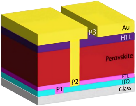
Process Flow for P1-P2-P3 Lithography in Series n-i-p Type PSM
Cleaned glass/ITO substrates undergo UV-O₃ treatment, followed by spin-coating of the SnO₂ electron transport layer (annealed at 150°C for 20 minutes). Subsequently, the ternary cationic perovskite layer is deposited using a two-step spin-coating method, with chloroform added prior to annealing to induce crystallization. The hole transport layer comprises PVK and CuInS₂ nanoparticle ink. Finally, a 75 nm metal electrode is deposited via thermal evaporation.
P1, P2, P3 Laser Etching Information
This study investigates the etching steps for P1, P2, and P3 in rigid and flexible TCO substrates with SnO₂/PSK/Spiro-OMeTAD/Au structures using a nanosecond ultraviolet laser (355 nm). It analyzes the effects of varying etching parameters on the morphology and contour of P1, P2, and P3 etched lines.
P1 Etching: Analysis of TCO Etch Performance
Interference fringes generated by glass substrate reflection may damage the TCO layer; reducing power can mitigate this issue.
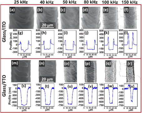
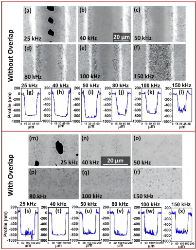
SEM images and profiles of scratch patterns (P1) on glass/ITO and glass/FTO samples (a–f: glass/ITO; m–r: glass/FTO)
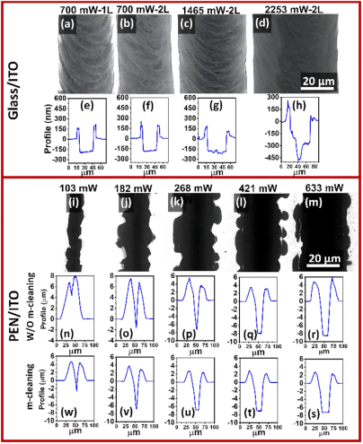
(a–d) SEM images of single and repeated scratches on glass/ITO at different Pₐᵥₑ values; (e–h) corresponding profilograms; (i–m) SEM images of PEN/ITO at different Pₐᵥₑ values; (n–r) profilograms before mechanical cleaning; (s–w) profilograms after mechanical cleaning
Glass/FTO substrate (thickness >600 nm): Under conditions of 25-80 kHz repetition frequency and 675 mW average power, etched stripes with sharp edges and no significant material buildup can be obtained.
Glass/ITO Substrate (Thickness ~200 nm): Low frequencies (25 kHz) may cause laser energy concentration, leading to localized overheating and microcracks on the substrate, with slight edge bulging (100-200 nm).
Flexible PEN/ITO Substrate: Average power must be controlled below 633 mW, combined with mechanical cleaning to reduce edge height from 8000 nm to 4000 nm.
P2 Scribing: ETL/PSK/HTL Scribing Performance Analysis
(a–f) SEM images of P2 single-line scribing at different repetition frequencies; (g–l) corresponding contour plots; (m–x) SEM images and contour plots of P2 stripes with 200 μm width and 10 μm grating pitch at different scan counts
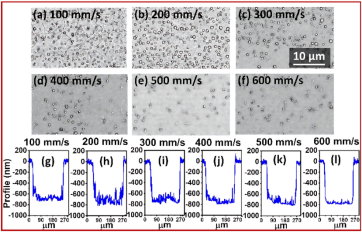
(a) to (f) SEM images of the perovskite layer (P2) scribed on a glass/ITO/SnO₂ structure
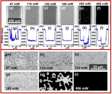
(a–f, m–r) SEM images of P2 scribing at different Pₐᵥₑ (47–406 mW); (g–l) corresponding contour plots
Ultraviolet laser (355 nm) exhibits high selectivity due to high absorption in the perovskite layer and low absorption in the TCO, enabling precise removal without damaging the substrate. CO₂ infrared laser (10 μm) requires energy four orders of magnitude higher and is prone to damaging FTO, while 532 nm green laser performs well but necessitates combination with other wavelengths. At optimal parameters (Pₐᵥₑ=119–189 mW, Fₚ=80 kHz, speed=400 mm/s), P2 scribing completely removes the functional layer without damaging ITO.
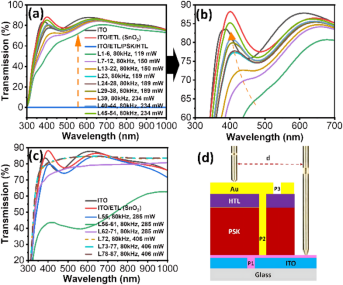
Transmission spectra of the glass/ITO/SnO₂/PSK/PVK/CuInS₂ structure before and after scribing
Transmission spectra reveal perovskite residues persist after multiple etching cycles at 150 mW power; at ≥234 mW, ITO damage increases but residues decrease. The optimal window is 150–234 mW (80 kHz, 400 mm/s).
P3 Etching: Au Back Electrode Etching Performance Analysis
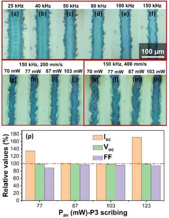
Optical microscope images of Au thin film (P3) etching under different parameters
Etching of the gold layer (75 nm) requires avoidance of edge delamination and damage to the underlying perovskite layer. Clear insulating trenches are obtained at a frequency of 100–150 kHz and a power of approximately 100 mW. Relative values of Iₛc, Vₒc, and FF for the segmented cells validate the etching effectiveness.
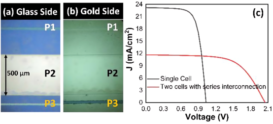
Optical images of the P1P2P3 pattern on (a) the glass side and (b) the gold side; (c) J-V curves of a single cell and a series-interconnected double cell
The J-V curves of the complete P1-P2-P3 pattern and the series-connected cell are shown. The Vₒc value approaches twice that of a single cell, confirming successful interconnection.
Nanosecond ultraviolet laser (355 nm) precisely controls thermal input by adjusting repetition rate (e.g., P2 recommends 80 kHz), average power (P2 suggests 119–189 mW), and scanning speed (e.g., 400 mm/s) precisely controls thermal input to avoid underlying damage, edge melting, or material residue. This enables P1-P2-P3 scribing for series interconnection in perovskite solar modules. Characterization of scribing morphology and quality demonstrates excellent repeatability in series interconnection, providing a reliable solution for perovskite module industrialization.
Millennial Perovskite Online Imaging Microscope
email:market@millennialsolar.com
The Millennial Perovskite Online Imaging Microscope is a precision measurement instrument based on CCD digital imaging and computer image technology. It performs high-magnification optical imaging of objects through an optical microscope, then transmits the images to a computer via a CCD camera system for measurement and analysis. This enables online detection of P1/P2/P3 laser scribing dimensions and defects.
• Multi-functional: Integrated size recognition and surface defect detection
• Enhanced precision: Achieves ±3μm accuracy for line width and spacing
• Faster inspection speed: Single-point size detection ≤3.5s, line scan for front-side cells ≤120s
• Database Support: Automatically annotates image dimensions and generates ECL data files for easy access by R&D personnel
Utilizing Millennial perovskite online imaging microscope with high-magnification optics and CCD digital imaging technology, this system performs real-time precision measurement and analysis of scribing morphology. It significantly enhances the repeatability and reliability of scribing processes, accelerating the industrialization of perovskite modules.
Related Products


