
Quantum Efficiency Tester
PL/EL Integrated System
PV-Reflectumeter
3D Confocal Microscope
In-Line Four Point Probe Tester
Four Point Probe Tester
In-Line Thin Film Thickness Tester
Raman Spectrometer
FTIR Spectrometer
Spectrophotometer
Automatic Spectroscopic Ellipsometer
Contact Resistance Tester
Ultra depth of field 3D microscope
Auto Visual Tester
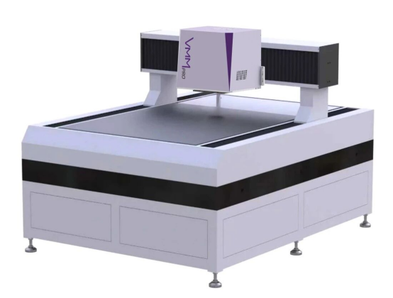
VMM PV Vision Measuring Machine
Solar Cell Horizontal Tensile Tester
Steady State Solar Simulator for Solar Cell
Solar Cell UV Aging Test Chamber
Solar Cell Comprehensive Tensile Tester
Visual Inspection Tester
Wet Leakage Current Tester
PV Module EL Tester
PV Module UV Preconditioning Chamber
Steady State Solar Simulator for PV Module
Current Continuous Monitor
Potential Induced Degradation Test
Bypass Diode Tester
LeTID Test System
Reverse Current Overload Tester
Impulse Voltage Tester
Hipot Insulation Tester
Ground Continuity Tester
Hipot Insulation Ground Tester
Damp Heat Test Chamber
Humidity Freeze Test
Thermal Cycle Test Chamber
Dynamic Mechanical Load Tester
Static Mechanical Load Tester
Hail Impact Tester
Robustness of Termination Tester
Module Breakage Tester
Cut Susceptibility Tester
Peel Shear Strength Tester
Universal Testing Machine (Single-arm)
Universal Testing Machine (Double-arm)
Glass Transmittance Tester
Acetic Acid Test Chamber
EVA Degree of Crosslinking Test System
Junction Box Comprehensive Tester
Drop ball tester
Semi-automatic scanning four-probe tester
Stylus Profilometer
Maximum Power Point Tracker
Perovskite Glass Transmittance Tester
Perovskite P1 Laser Scribing Multifunctional Testing Machine
Perovskite Online PL Tester
Perovskite Online Sheet Resistance Tester
Online Perovskite Film Thickness Tester
Perovskite Process Inspection Workstation
Portable EL Tester
Portable Thermal Imaging Tester
Solar Module Multi-Channel Testing System
PV Inverter Power Quality Tester
Drone EL Tester
IV Tester
IVEL Cell Sorting Machine
Perovskite Solar Cell Module P1-P2-P3 Laser Scribing Process Achieves Efficient Interconnection and Minimized Dead Zones
Date : 19 January 2026Views : 2295
During the fabrication of series-connected perovskite solar cells, precise scribing is required for different functional layers. Current patterning methods include stencil masking, chemical etching, mechanical scribing, and laser scribing. Laser scribing is increasingly becoming the mainstream technique due to its ability to achieve higher precision in patterning. The Millennial Perovskite Large-Area Imaging Tester was introduced to enable real-time monitoring and intelligent analysis of scribing morphology, material residue, and interface quality.
This study employed a fiber-based femtosecond laser system with a wavelength of 532 nm and a pulse width of 300 fs to successfully complete the preparation of all P1, P2, and P3 scribing lines. Through process parameter optimization, the optimal parameters for P1 scribing were determined as a scribing speed of 2000 mm/s and a laser power of 1.8 W, achieving high-quality scribing with a slit width less than 10 μm. The results demonstrate that laser scribing technology holds significant application value in enhancing the interconnection performance of perovskite solar cell modules.
Experimental Section
Materials
The laser-patterned perovskite module consists of three layers: P1, P2, and P3.
P1 layer: ITO glass with a thickness of approximately 500 nm.
P2 layer: A hybrid film layer approximately 800 nm thick, comprising SnO₂ (ETL), FA₀.₉₅Cs₀.₀₅PbI₃ perovskite absorber layer, and Spiro-OMeTAD (HTL).
P3 layer: A nanoscale gold (Au) layer approximately 80 nm thick.
Experimental Setup
A femtosecond laser with a pulse width of 300 fs and a wavelength of 532 nm was selected, featuring a maximum average power of 40 W and a maximum repetition rate of 500 kHz. The beam diameter is 2 mm, utilizing a 2–10× beam expander. The laser operates in either single-pulse or pulse-train mode (adjustable from 1 to 10 pulses). The beam is vertically incident on the sample, which is positioned on an XY motorized stage with micrometer-level positioning accuracy.
Characterization Methods
Video microscopy is employed to observe the microstructure and morphology of the samples. Laser confocal microscopy is used for section-by-section 3D imaging and scratch depth measurement. A digital multimeter is utilized to measure the resistivity of the samples.
P1 Scratch Process Optimization
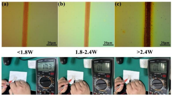
Laser P1 Scribing Microscope Images and Resistance Measurement Diagrams at Different Power Ranges
The objective of P1 scribing is to completely remove the ITO layer without damaging the glass substrate. When laser power is below 1.8 W, scribing is incomplete, with both sides remaining conductive (17.3 Ω). Power exceeding 2.4 W causes substrate damage, resulting in black scorched areas. Within the 1.8–2.4 W range, clear isolation is achieved without substrate damage.
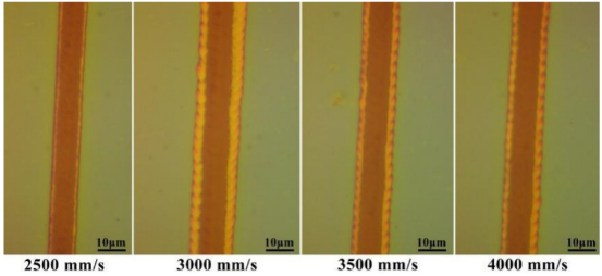
Microscopic images of the P1 marking area at different laser marking speeds
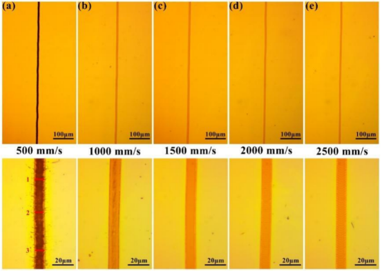
Microscopic images of P1 marking at different speeds with a laser power of 2.4W
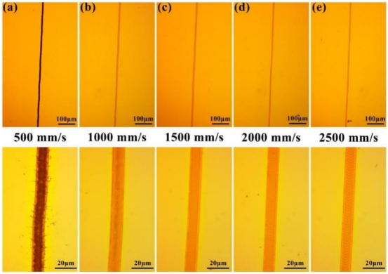
Microscopic images of P1 marking at different speeds with a laser power of 2.1W
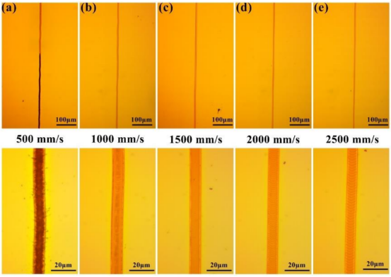
Microscopic images of P1 marking at different speeds with a laser power of 1.8W
Scribing speed also significantly impacts processing quality. When speeds exceed 2500 mm/s, the heat-affected zone noticeably increases; therefore, speeds should be maintained below 2500 mm/s. Under fixed power settings of 2.4 W, 2.1 W, and 1.8 W, scribing effects were tested across a speed range of 500–2500 mm/s.
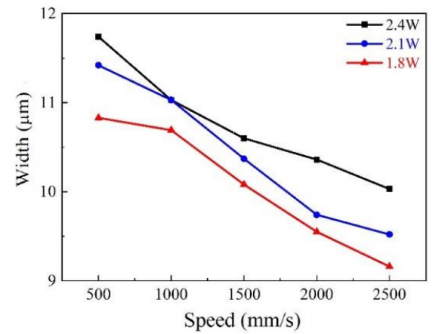
Relationship between Scribing Width and Processing Speed for P1
Results indicate that as speed increases, the scribing morphology transitions from coarse, torn edges to uniform striations. Average seam widths decrease from 11.74 μm, 11.42 μm, and 10.83 μm to 10.03 μm, 9.52 μm, and 9.16 μm, respectively. Significant heat-affected zones were observed at 500 mm/s, while under other conditions, the heat-affected zone width was controlled within 1 μm.
Considering the combined effects of power and speed, the optimal process parameters for P1 were determined as: power 1.8 W, speed 2000 mm/s, frequency 1000 kHz, single-pulse mode, and zero defocus. Under these conditions, the minimum seam width and controllable heat-affected zone were achieved, meeting the stringent requirements for “dead zone” width in high-efficiency modules.
P2 Scribing Process
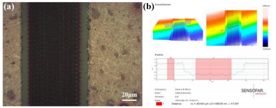
(a) Microscopic image and (b) 3D imaging depth test diagram of laser P2 scribing
P2 requires penetration through the Perovskite/HTL/Au multilayer structure without damaging the P1 layer's ITO, presenting the highest technical difficulty. The experiment employed a filled scribing pattern (line width 100 μm) at a power of 0.46 W and a speed of 4000 mm/s, achieving a scribing depth of 858 nm. This precisely removed the entire P2 layer without damaging the underlying ITO.
P3 scribing process
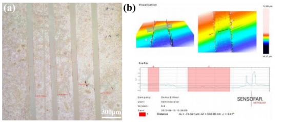
(a) Microscopic image and (b) 3D imaging depth test map of laser P3 scribing
P3 requires removal of gold electrodes and isolation of adjacent cells. Optimized parameters are power 0.2 W, speed 6000 mm/s, and scribing depth 534 nm. Though slightly deeper than the gold layer thickness, it does not damage the P1 layer, meeting electrical isolation requirements.
This study systematically optimized the femtosecond laser scribing process for perovskite solar cell modules. It established that P1 scribing should be performed within the power range of 1.8–2.4 W and at speeds below 2500 mm/s to achieve complete ITO layer isolation while avoiding glass substrate damage. Additionally, increasing speed or reducing power effectively minimized slot width and heat-affected zones. The final optimal parameters for P1 were determined as: speed of 2000 mm/s, and frequency of 1000 kHz in single-pulse mode. P2 and P3 scribing achieved precise etching without damaging underlying structures at 0.46 W/4000 mm/s and 0.2 W/6000 mm/s, respectively. This process provides a reliable technical pathway for achieving efficient interconnections and minimizing dead zones in perovskite modules.
Millennial Perovskite Large-Area Imaging Tester
The Millennial Perovskite Large-Area Imaging Tester is a precision measurement instrument based on CCD digital imaging and microscopic imaging technology. It performs high-magnification optical magnification imaging of objects through an optical microscope, then transmits the images to a computer via a CCD camera system for measurement and analysis. It enables online detection of P1/P2/P3 laser scribing dimensions and defects.
email:market@millennialsolar.com
• Multi-functional: Integrated dimension recognition + surface defect detection
• Enhanced precision: Achieves ±3μm accuracy for line width and spacing
• Accelerated inspection speed: Single-point dimension detection ≤3.5s, full-cell scanning <120s
• Database support: Automatically annotates image dimensions and generates ECL data documents for easy access by R&D personnel
Utilizing Millennial perovskite large-area imaging tester with high-magnification optical zoom and CCD digital imaging technology, it performs real-time precision measurement and analysis of scribing morphology. This significantly enhances the repeatability and reliability of scribing processes, driving the industrialization of perovskite modules.
Related Products


