
Quantum Efficiency Tester
PL/EL Integrated System
PV-Reflectumeter
3D Confocal Microscope
In-Line Four Point Probe Tester
Four Point Probe Tester
In-Line Thin Film Thickness Tester
Raman Spectrometer
FTIR Spectrometer
Spectrophotometer
Automatic Spectroscopic Ellipsometer
Contact Resistance Tester
Ultra depth of field 3D microscope
Auto Visual Tester
VMM PV Vision Measuring Machine
Solar Cell Horizontal Tensile Tester
Steady State Solar Simulator for Solar Cell
Solar Cell UV Aging Test Chamber
Solar Cell Comprehensive Tensile Tester
Visual Inspection Tester
Wet Leakage Current Tester
PV Module EL Tester
PV Module UV Preconditioning Chamber
Steady State Solar Simulator for PV Module
Current Continuous Monitor
Potential Induced Degradation Test
Bypass Diode Tester
LeTID Test System
Reverse Current Overload Tester
Impulse Voltage Tester
Hipot Insulation Tester
Ground Continuity Tester
Hipot Insulation Ground Tester
Damp Heat Test Chamber
Humidity Freeze Test
Thermal Cycle Test Chamber
Dynamic Mechanical Load Tester
Static Mechanical Load Tester
Hail Impact Tester
Robustness of Termination Tester
Module Breakage Tester
Cut Susceptibility Tester
Peel Shear Strength Tester
Universal Testing Machine (Single-arm)
Universal Testing Machine (Double-arm)
Glass Transmittance Tester
Acetic Acid Test Chamber
EVA Degree of Crosslinking Test System
Junction Box Comprehensive Tester
Drop ball tester
Semi-automatic scanning four-probe tester
Stylus Profilometer
Maximum Power Point Tracker
Perovskite Glass Transmittance Tester
Perovskite P1 Laser Scribing Multifunctional Testing Machine
Perovskite Online PL Tester
Perovskite Online Sheet Resistance Tester
Online Perovskite Film Thickness Tester
Perovskite Process Inspection Workstation
Portable EL Tester
Portable Thermal Imaging Tester
Solar Module Multi-Channel Testing System
PV Inverter Power Quality Tester
Drone EL Tester
IV Tester
IVEL Cell Sorting Machine
Optimization of SiNx Antireflection and Passivation Layer Deposition: Balancing Hydrogen Content and Si-N Bond Density
Date : 13 March 2026Views : 1005
In the industrial manufacturing of crystalline silicon solar cells, silicon nitride (SiNx) films deposited via plasma-enhanced chemical vapor deposition (PECVD) serve as a core multifunctional layer combining antireflection, surface passivation, and bulk passivation functions. The realization of its outstanding surface passivation performance is fundamentally constrained by the mutual trade-off between hydrogen content and the compactness of the Si-N bond network within the film. This paper analyzes the microscopic mechanism of this contradiction from the perspectives of quantum mechanics, surface physics, and film growth kinetics, systematically elaborating the theoretical pathways and engineering strategies for achieving the optimal balance between these two factors in industrial PECVD processes.
I. The Dual Mission of SiNx Films and the Physical Roots of Performance Conflict
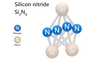
SiNx thin film
SiNx films must simultaneously achieve two core objectives: reducing surface recombination rates to enhance carrier lifetime, and constructing a dense, stable structure to resist contamination and oxidation of the underlying silicon substrate. The fundamental contradiction lies in: high hydrogen dilution promotes Si-H bond formation for efficient passivation but reduces Si-N network crosslinking; conversely, high density requires strengthening Si-N bonds and reducing hydrogen content, yet this increases dangling bonds on the silicon surface.
1. Optical Mission (Anti-Reflection)
As an ideal anti-reflective layer, its refractive index must achieve impedance matching with both the silicon substrate and air. By regulating the Si/N ratio, the refractive index can be precisely controlled within the ideal range of 2.0–2.1, demanding uniform and controllable chemical composition of the film.
2. Electrical Mission (Passivation)
Passivation is the core value of the SiNx layer, achieved through two mechanisms: Chemical passivation saturates silicon surface dangling bonds and reduces interface state density; Field-effect passivation utilizes fixed positive charges within the film to repel minority carriers via Coulombic forces, thereby suppressing surface recombination.
The core contradiction stems from hydrogen's dual role: On one hand, hydrogen acts as a “passivation agent”—the Si-H and N-H bonds it forms are essential for hydrogen release, diffusion, and defect repair within the silicon substrate during subsequent sintering. High hydrogen content is the material foundation for efficient passivation. On the other hand, hydrogen acts as a “structural disruptor.” An abundance of Si-H and N-H bonds (with bond energies far below Si-N bonds) disrupts the continuity of the Si-N three-dimensional network. This leads to reduced film density and stability, decreased fixed charge density, and weakened field-effect passivation effects. Therefore, optimizing SiNx deposition fundamentally involves seeking a Pareto optimum between hydrogen's passivation capability and the stability of the Si-N network.
II. Correlation Mechanism Between Microstructural Bonding and Macro-level Properties
1. Hydrogen Existence State and Passivation Efficiency
The form of hydrogen in the film directly determines passivation efficiency: Si-H bonds (FTIR characteristic peak ~2160–2200 cm⁻¹, bond energy ~3.1 eV) effectively passivate silicon defects with superior thermal stability compared to N-H bonds (FTIR characteristic peak ~3340 cm⁻¹). Optimized SiNx films require not only moderate total hydrogen content but also enhanced Si-H/N-H bond ratios to improve hydrogen utilization efficiency and film thermal stability.
2. Density and Stability of Si-N Bond Network
The peak position and full width at half maximum (FWHM) of the Si-N bond stretching vibration mode (~840 cm⁻¹) are core indicators of network density. A shift toward higher wavenumbers and narrower FWHM indicate a more stable and uniform Si-N bonding network. A dense network endows the film with high mechanical hardness, corrosion resistance, excellent PID resistance, stable charge trapping, and low light absorption characteristics, ensuring long-term reliability and photovoltaic performance of the cell.
III. PECVD Deposition Parameters: The Core Means of Balancing Control
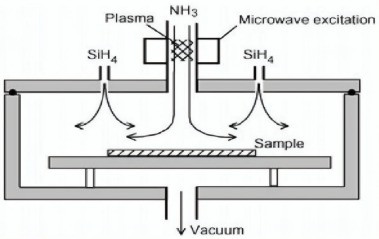
Principles of PECVD
The PECVD process achieves precise control over the microstructure of SiNx films by accurately regulating key parameters, thereby balancing hydrogen content and Si-N bond density.
1. Silane to Ammonia Flow Ratio (NH₃/SiH₄)
This parameter is central to controlling the Si/N stoichiometric ratio and hydrogen bonding pattern. A high NH₃/SiH₄ ratio produces nitrogen-rich films (SiNx, x > 1.33) with elevated hydrogen content but low Si-H bond proportion, resulting in poor density. A low NH₃/SiH₄ ratio yields silicon-rich films (SiNx, x<1.33), increasing the Si-H bond ratio but also boosting optical absorption and reducing fixed charge density. The optimal range is a narrow window requiring precise calibration through FTIR and minority carrier lifetime measurements.
2. Deposition Temperature
Temperature governs film growth kinetics: Low temperatures (<400°C) cause insufficient precursor surface migration, forming loose porous structures with high hydrogen content but extremely poor stability; High temperatures (>450°C) promote dense cross-linked Si-N networks, reducing hydrogen content and favoring stable Si-H bonds, but insufficient total hydrogen may impair bulk passivation after sintering. The optimization strategy involves employing higher deposition temperatures while supplementing essential hydrogen content through gas ratio adjustments, all while avoiding thermal damage to the silicon substrate and p-n junction (typically <500°C).
3. RF Power and Reaction Chamber Pressure
These factors synergistically determine plasma characteristics: High RF power enhances film density through ion bombardment, but excessively high power introduces lattice damage and weak bond breakage; Low pressure increases ion energy, while high pressure boosts plasma density but reduces ion energy, leading to film porosity. The current frontier approach employs a “high-density, low-energy” plasma mode, ensuring deposition rates while avoiding bombardment damage to achieve high-quality, efficient deposition.
IV. Theoretical Pathways and Outlook for Achieving Ultimate Balance
Ideal SiNx:H films should exhibit a microstructure that combines rigidity and flexibility: a highly cross-linked, dense, and stable three-dimensional Si-N bond network serves as a rigid framework, providing mechanical stability and field-effect passivation capability. Embedding an appropriate amount of hydrogen atoms, primarily via Si-H bonds, at framework nodes or voids allows these atoms to be activated and released during sintering, thereby repairing silicon defects.
Future optimization will advance toward intelligent, microscopic upgrades: First, in-situ diagnostics and real-time control, integrating in-situ ellipsometer spectroscopy and mass spectrometry for closed-loop regulation during film growth. Second, multilayer/gradient structure design, achieving both passivation and protective properties through interfaces enriched with silicon and Si-H bonds, while outer layers maintain nitrogen-rich density. Third, precursor engineering will explore advanced silicon sources to achieve high-performance films at lower temperatures.
Optimizing SiNx film deposition is an atomic-scale balancing act requiring profound understanding of hydrogen's dual roles. By precisely controlling the PECVD process, we must identify the optimal equilibrium between hydrogen content and Si-N bond density to maximize both cell conversion efficiency and long-term reliability. This represents both an engineering challenge and a significant research frontier in materials science.


