
Quantum Efficiency Tester
PL/EL Integrated System
PV-Reflectumeter
3D Confocal Microscope
In-Line Four Point Probe Tester
Four Point Probe Tester
In-Line Thin Film Thickness Tester
Raman Spectrometer
FTIR Spectrometer
Spectrophotometer
Automatic Spectroscopic Ellipsometer
Contact Resistance Tester
Ultra depth of field 3D microscope
Auto Visual Tester
VMM PV Vision Measuring Machine
Solar Cell Horizontal Tensile Tester
Steady State Solar Simulator for Solar Cell
Solar Cell UV Aging Test Chamber
Solar Cell Comprehensive Tensile Tester
Visual Inspection Tester
Wet Leakage Current Tester
PV Module EL Tester
PV Module UV Preconditioning Chamber
Steady State Solar Simulator for PV Module
Current Continuous Monitor
Potential Induced Degradation Test
Bypass Diode Tester
LeTID Test System
Reverse Current Overload Tester
Impulse Voltage Tester
Hipot Insulation Tester
Ground Continuity Tester
Hipot Insulation Ground Tester
Damp Heat Test Chamber
Humidity Freeze Test
Thermal Cycle Test Chamber
Dynamic Mechanical Load Tester
Static Mechanical Load Tester
Hail Impact Tester
Robustness of Termination Tester
Module Breakage Tester
Cut Susceptibility Tester
Peel Shear Strength Tester
Universal Testing Machine (Single-arm)
Universal Testing Machine (Double-arm)
Glass Transmittance Tester
Acetic Acid Test Chamber
EVA Degree of Crosslinking Test System
Junction Box Comprehensive Tester
Drop ball tester
Semi-automatic scanning four-probe tester
Stylus Profilometer
Maximum Power Point Tracker
Perovskite Glass Transmittance Tester
Perovskite P1 Laser Scribing Multifunctional Testing Machine
Perovskite Online PL Tester
Perovskite Online Sheet Resistance Tester
Online Perovskite Film Thickness Tester
Perovskite Process Inspection Workstation
Portable EL Tester
Portable Thermal Imaging Tester
Solar Module Multi-Channel Testing System
PV Inverter Power Quality Tester
Drone EL Tester
IV Tester
IVEL Cell Sorting Machine
Loss Analysis of the Perovskite Solar Cell Scribing Process Based on Hyperspectral Photoluminescence (PL) Imaging
Date : 18 March 2026Views : 1380
The large-scale application of perovskite solar cells (PSCs) relies on precision laser scribing for series interconnection and requires spatial characterization of cell parameters to understand the interaction between the laser and the material. This study focuses on the P3 scribing step and investigates the processing effects of nanosecond (ns) and picosecond (ps) laser pulses at different pulse energies. Using high-resolution imaging from a large-format perovskite cell photoluminescence (PL) tester, the spatial distributions of key parameters—including optical bandgap, Urbach energy, and shunt resistance—were mapped and analyzed in conjunction with electrical measurement data. The results indicate that, under optimized pulse energy, both types of lasers can achieve effective series interconnection with minimal performance loss. This provides important evidence for the applicability of laser patterning technology in the industrial-scale production of perovskite modules.
Materials and Methods
Sample Preparation
Sample preparation followed standard perovskite fabrication procedures, including: ITO transparent front electrode deposition, P1 laser scribing, cleaning, SnO₂ electron transport layer preparation, perovskite absorber spin coating, hole transport layer spin coating, P2 laser scribing, gold back electrode evaporation, and P3 laser scribing.
Laser Scribing
The laser processing system is equipped with picosecond and nanosecond laser sources. Parameters P1 and P2 remain constant, while step P3 employs three different energy input conditions (low, optimal, and high). During the scribing process, samples are processed in a nitrogen atmosphere to minimize degradation and debris generation.
PL and Electrical Performance Characterization
A hyperspectral PL imaging system was used, employing continuous-wave lasers at 405 nm and 532 nm for excitation, with a spatial resolution of approximately 1 μm and a spectral resolution better than 2.5 nm. Electrical performance testing utilized an AAA-grade solar simulator to record J-V curves.
Analysis of PL Intensity and Center Wavelength
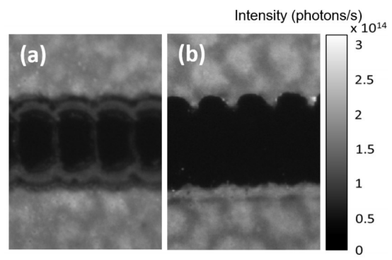
Images of the photoluminescence flux (photons/s) of perovskite samples: (a) etched with ns laser pulses, with an optimal irradiation dose of 1.36 J/cm²; (b) etched with ps laser pulses, with an optimal irradiation dose of 2.31 J/cm²
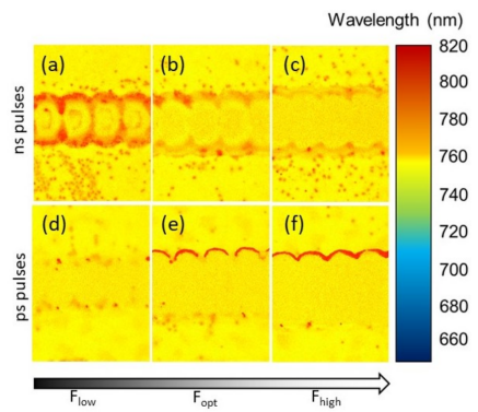
Spatially resolved images of the wavelength of localized photoluminescence emission from perovskite samples: (a–c) samples etched with ns laser pulses; (d–f) samples etched with ps laser pulses. All images cover three dose ranges: (a, d) low dose; (b, e) optimal dose; (c, f) high dose.
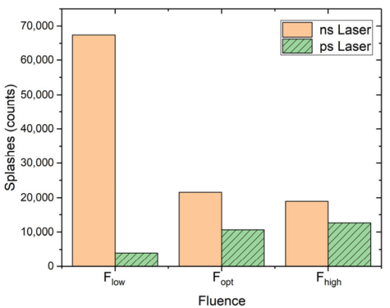
Comparison of the amount of sputtered material observed along the laser etching line as a function of the applied dose during ns and ps laser pulse etching. The width of the analysis region near the groove matches the width of the corresponding groove
At the optimal injection dose, uniform PL emission was observed near 758 nm, corresponding to a bandgap of approximately 1.64 eV. The PL signal detected within the etched grooves originated from residual absorbed layer material but did not affect electrical functionality. A distinct red shift appeared at the edges of the etched lines, attributed to material changes and the condensation of sputtered material caused by explosive boiling. The ps laser outperformed the ns laser in terms of material removal efficiency.
Urbach energy analysis
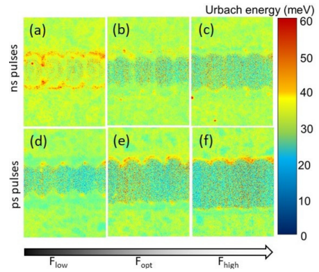
Spatially resolved images of the local Ulbach energy in perovskite samples: (a–c) show samples etched by ns laser pulses, and (d–f) show samples etched by ps laser pulses
The Urbach energy (Eᵤ) directly reflects the density of trap states in perovskites. At low irradiation doses, Eᵤ increases with ns lasers, possibly due to incomplete material removal; whereas at high irradiation doses, ps lasers cause increased damage to the top edge due to the non-Gaussian beam distribution. Both lasers are suitable for P3 scribing at optimized irradiation doses.
Bypass resistance analysis
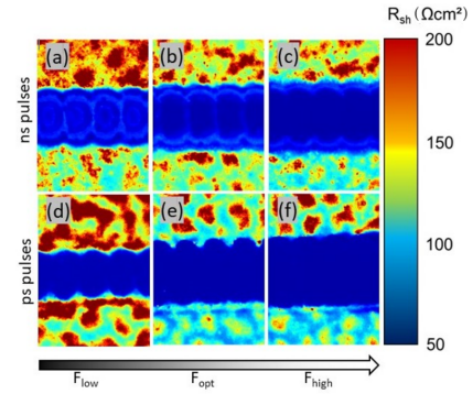
Spatially resolved images of the local shunt resistance (Rₛₕ) in perovskite samples: (a–c) samples etched by ns laser pulses; (d–f) samples etched by ps laser pulses
The local shunt resistance derived from PL images reveals island-like high-resistance regions at the etched edges, which may be related to material degradation caused by the separation of bromide and iodide phases. There is no significant difference in Rₛₕ between ns and ps lasers.
Electrical Performance Analysis
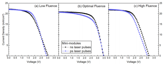
Current-Voltage (J-V) Curves of Three-Segment Micro-Modules Etched Using ns and ps Laser Pulses
The J-V curves indicate that effective series interconnection can be achieved under various pulse energy conditions. Performance degradation at low pulse energies results from insufficient material removal, while at high pulse energies, it stems from overheating and excessive ablation. Optimal performance is achieved at the optimal pulse energy, particularly with the ns laser.
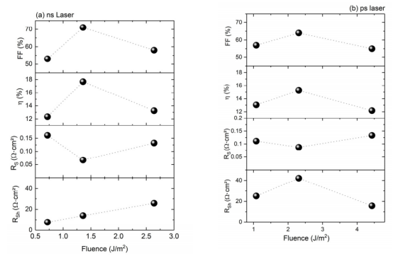
Plots of FF, η, Rₛ, and Rₛₕ as a function of injection current for perovskite samples etched by ns laser pulses (a) and ps laser pulses (b)
Parameters extracted from the J-V curves indicate that the fill factor and conversion efficiency are highest at the optimal injection current, while the series resistance remains low and stable, suggesting that the ITO layer is undamaged.
This study analyzed the effects of nanosecond and picosecond lasers on the perovskite layer during P3 patterning using hyperspectral PL imaging. The results show that both lasers can achieve effective patterning, and the perovskite is insensitive to the thermal effects of the laser. The influence of dose on electrical parameters is more significant than that of pulse duration, and the process window is wide, allowing for tolerance to fluctuations in production conditions, making it suitable for large-scale manufacturing.
Large-Platform Perovskite Solar Cell PL Tester
The Large-Platform Perovskite Solar Cell PL Tester systematically addresses core challenges in solar cell production—such as speed, yield, cost, process optimization, and stability—through its non-contact, high-precision, and real-time feedback capabilities. Combined with AI deep learning, it enables fully automated defect detection and process feedback.
email:market@millennialsolar.com
▶ High-Precision PL Imaging: Utilizes a line-scan laser with imaging accuracy < 75 μm/pixel (imaging accuracy is customizable)
▶ Supports 16-bit grayscale: Clearly displays both high-brightness areas (e.g., defect-free zones) and low-brightness areas (e.g., dark defect spots) simultaneously
▶ High-Speed In-Line PL Defect Detection: Detection speed ≤ 2 s, false negative rate < 0.1%; false positive rate < 0.3%
▶ AI defect recognition and classification training: Enables fully automated defect recognition and process feedback
The large-platform perovskite cell PL tester effectively evaluates local material changes in the scribed areas, which are related to interconnection quality and cell performance. This study provides important evidence for optimizing the laser scribing process for industrial-grade perovskite modules.
Related Products


