
Quantum Efficiency Tester
PL/EL Integrated System
PV-Reflectumeter
3D Confocal Microscope
In-Line Four Point Probe Tester
Four Point Probe Tester
In-Line Thin Film Thickness Tester
Raman Spectrometer
FTIR Spectrometer
Spectrophotometer
Automatic Spectroscopic Ellipsometer
Contact Resistance Tester
Ultra depth of field 3D microscope
Auto Visual Tester
VMM PV Vision Measuring Machine
Solar Cell Horizontal Tensile Tester
Steady State Solar Simulator for Solar Cell
Solar Cell UV Aging Test Chamber
Solar Cell Comprehensive Tensile Tester
Visual Inspection Tester
Wet Leakage Current Tester
PV Module EL Tester
PV Module UV Preconditioning Chamber
Steady State Solar Simulator for PV Module
Current Continuous Monitor
Potential Induced Degradation Test
Bypass Diode Tester
LeTID Test System
Reverse Current Overload Tester
Impulse Voltage Tester
Hipot Insulation Tester
Ground Continuity Tester
Hipot Insulation Ground Tester
Damp Heat Test Chamber
Humidity Freeze Test
Thermal Cycle Test Chamber
Dynamic Mechanical Load Tester
Static Mechanical Load Tester
Hail Impact Tester
Robustness of Termination Tester
Module Breakage Tester
Cut Susceptibility Tester
Peel Shear Strength Tester
Universal Testing Machine (Single-arm)
Universal Testing Machine (Double-arm)
Glass Transmittance Tester
Acetic Acid Test Chamber
EVA Degree of Crosslinking Test System
Junction Box Comprehensive Tester
Drop ball tester
Semi-automatic scanning four-probe tester
Stylus Profilometer
Maximum Power Point Tracker
Perovskite Glass Transmittance Tester
Perovskite P1 Laser Scribing Multifunctional Testing Machine
Perovskite Online PL Tester
Perovskite Online Sheet Resistance Tester
Online Perovskite Film Thickness Tester
Perovskite Process Inspection Workstation
Portable EL Tester
Portable Thermal Imaging Tester
Solar Module Multi-Channel Testing System
PV Inverter Power Quality Tester
Drone EL Tester
IV Tester
IVEL Cell Sorting Machine
Silver-on-Copper Technology in Photovoltaic Cell Manufacturing
Date : 20 March 2026Views : 930
In the field of photovoltaic cell manufacturing, the silver-on-copper technology for crystalline silicon cells is a critically important core process. By uniformly depositing a layer of silver of appropriate thickness onto the surface of a copper electrode, this technology retains the high electrical conductivity and excellent contact properties of silver electrodes while significantly reducing the amount of the precious metal silver used, thereby substantially lowering overall material costs. This innovative approach not only effectively improves the photovoltaic conversion efficiency of cells and enhances the output performance of modules, but also helps reduce reliance on scarce resources, promotes the optimization of material utilization, and facilitates cost control across the industrial chain. Consequently, it provides a solid technological foundation and economic viability for the large-scale application and sustainable development of the solar industry.
I. Principles of Silver-Coated Copper Technology
Copper-plated silver technology
Silver-Coated Copper (SCC) technology is a metallization paste technology whose primary objective is to significantly reduce the amount of the precious metal silver used, while maintaining or approaching the conductivity and solderability of pure silver paste. The basic principle involves using copper as the core material (main body) and uniformly coating its surface with a thin layer of silver.
Core Material: High-purity copper powder is used as the main conductive material. Copper’s electrical conductivity is second only to silver (approximately 95% IACS vs. silver’s 105% IACS), yet its price is significantly lower than silver’s (historically, silver prices have typically been 70–100 times higher than copper prices), making it an ideal substitute.
Coating Material: Pure silver is used as the coating layer. Silver offers the best electrical conductivity, excellent oxidation resistance, and good weldability.
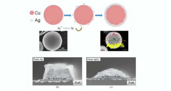
Coating Process: This is the core of the technology. Typically, a dense, nanoscale silver layer is uniformly deposited on the surface of the copper powder particles through electroless plating or displacement plating.
Electrolytic Plating: A reducing agent (such as hypophosphite, formaldehyde, or glucose) is used to reduce silver ions (Ag⁺) in the solution to silver atoms (Ag⁰) on the surface of the copper powder, which are then deposited. This process requires strict control of parameters such as temperature, pH, and concentration to ensure the plating layer is uniform, dense, and free of pores.
Displacement plating: This method utilizes the standard electrode potential difference between copper and silver (Cu²⁺/Cu = +0.34 V, Ag⁺/Ag = +0.80 V). When copper powder is immersed in a silver salt solution (such as silver nitrate), the copper spontaneously dissolves (oxidizing to Cu²⁺), while silver ions are reduced and deposited onto the copper surface. This method is relatively simple, but controlling coating thickness and uniformity requires greater skill.
Slurry Preparation: Coated silver-on-copper powder (Ag@Cu) is mixed, ground, and dispersed with other slurry components (glass powder, organic carrier—including resin, solvent, and rheology modifiers) to produce a conductive slurry suitable for screen printing.
Sintering process: During the final sintering stage of cell manufacturing, the organic carrier is burned off, the glass powder melts, and the silicon nitride anti-reflective layer on the wafer surface is slightly etched, enabling the molten metal particles to form a good ohmic contact with the silicon (forming a silver-silicon alloy). At the same time, the molten metal particles interconnect to form low-resistance conductive grid lines. The key is that the silver layer remains intact and completely encapsulates the internal copper, preventing the copper from oxidizing or reacting adversely with the silicon at high temperatures.
Key Points: The silver layer must be continuous, dense, and free of defects to effectively isolate the internal copper, protecting it from oxidation or corrosion during paste preparation, storage, printing, sintering, and subsequent use in cells and modules.
II. Advantages of Silver-Clad Copper Technology
Significant Reduction in Material Costs: This is the core advantage. Replacing most of the expensive silver with inexpensive copper (typically accounting for over 90% of the composition) directly and substantially reduces paste costs. Silver consumption can typically be reduced by 30%–60% or even more (depending on the thickness of the cladding layer and the final silver content), making this one of the most effective ways to reduce non-silicon costs.
Excellent Electrical Conductivity: Since electrical conduction primarily occurs at the metal surface (Skin Effect), a dense, continuous silver coating provides conductivity comparable to that of pure silver paste, ensuring low resistance in the grid lines. The increase in the cell’s series resistance (Rs) is very limited and can even be controlled to be comparable to that of pure silver.
Solderability and reliability (potential): The surface silver layer ensures good solderability of the grid lines, facilitating subsequent bonding of the lead wires at the module end. Theoretically, a dense silver layer effectively isolates oxygen and moisture, preventing oxidation and corrosion of the internal copper and providing reliable long-term electrical performance.
High Process Compatibility: Silver-clad copper paste is similar in form to pure silver paste and can typically be produced using existing screen printing equipment and sintering processes. This eliminates the need for large-scale modifications to the cell manufacturing line, making it easy to implement.
Reduced Reliance on Silver Resources: As photovoltaic production capacity continues to expand, the demand for silver is enormous. Silver-clad copper technology helps mitigate the risks associated with silver supply pressures and price volatility.
III. Cost Advantages
Composition of Non-Silicon Costs: In the total cost of crystalline silicon solar cells, “non-silicon costs” refer to all costs other than those associated with silicon wafers. These primarily include: metallization pastes (front-side silver paste, back-side silver/aluminum paste), chemicals (texturing, diffusion, etching, coating, etc.), consumables (quartz boats, screens, gases, etc.), equipment depreciation, labor, and energy.
Silver Paste Is the Largest Single Cost Item: For a long time, the cost of front-side silver paste has consistently accounted for the largest share of non-silicon costs in crystalline silicon cells, typically reaching 25%–35% or even higher.
This is primarily due to:
High Silver Prices: Silver is a precious metal that is expensive and subject to significant price fluctuations.
Massive consumption: High-efficiency cells such as PERC and TOPCon require dense, fine, and highly conductive silver grid lines on the front side to collect current, resulting in significant silver consumption (currently, mainstream PERC cells use approximately 70–80 mg per wafer, while TOPCon cells use approximately 80–100 mg per wafer or even more).
High technical barriers: High-performance silver paste formulations are complex, subject to significant patent barriers, and supplied by a concentrated number of vendors.
The core value of silver-clad-copper technology: Precisely because front-side silver paste accounts for a massive proportion of costs, silver-clad-copper technology directly and significantly reduces silver consumption (by 30%–60%), offering the most direct and significant effect on lowering “non-silicon costs.” It achieves the most substantial reduction in non-silicon cost per watt while maintaining excellent cell performance.
By uniformly coating the surface of copper powder with a dense layer of silver, the silver-clad-copper technology organically combines the low-cost characteristics of copper with the excellent electrical properties of silver. It is currently the most effective and already large-scale industrialized technical approach for reducing the non-silicon costs of crystalline silicon solar cells (primarily the cost of front-side silver paste). The core advantages of this technology lie in its significant cost reduction and excellent process compatibility.


